
Videos
A.
Output voltage due to input bias current and worst case output voltage.
A.
Answer to Problem 14.50P
Output voltage due to input bias current is
Explanation of Solution
Given:
The given circuit is:
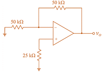
Input bias current
Input offset current
Let the general circuit with input bias currents
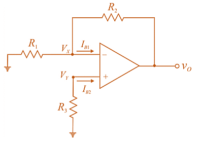
Now, using superposition determine
For
The output voltage due to
For
Since,
The output voltage due to
So, the vet output voltage due to both
If
So, the output voltage due to bias current
Now putting the values,
Now, for worst case output
As,
And
Adding (5) and (6)
From (5)
For
For
Assume
For the given circuit
Putting the values in (3)
So, including the effect of input offset current, the worst case output voltage is
B.
Output voltage due to input bias current and worst case output voltage.
B.
Answer to Problem 14.50P
Output voltage due to input bias current is
Explanation of Solution
Given:
The given circuit is:
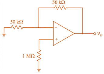
Input bias current
Input offset current
Considering equation 4.
Now, for worst case output voltage
Assume
For the given circuit
Putting the values in (3)
So, including the effect of input offset current, the worst case output voltage is
Want to see more full solutions like this?
Chapter 14 Solutions
Microelectronics: Circuit Analysis and Design


- 2. The bridge rectifier circuit has AC source Vrms=230V at 50Hz and there is a series RL load with R=50 Q and L=100mH in the output. (a) draw the circuit and draw input and output characteristic voltages and currents. (b) Determine the output average current.arrow_forwardBlock diagram reductionarrow_forwardQ4) If fr is the frequency of the fundamental component of the output ripple, then for full bridge rectifier, the output frequency fo in respect to input frequency fi is Ofr=fo=2fi Ob.fr=fo%3D3fi Ofr=fo=D4fi Ofr=fo=fiarrow_forward
- The positive peak value of output waveform for the given circuit diagram is.. . (VPP of input is 14 V, Bias voltage is 4 V, Diode is silicon) R1 I D, VIN VOut VELAS Earrow_forwardWhat is: Nyquist criterion marginsarrow_forwardwhat is the difference of MOSFET and Diode in Boost Converter. Can you also sight an example?arrow_forward
- Positive Clamper: The function of the 2 points positive clamper is to raise the input signal to upward direction such that negative peaks falls to ..'arrow_forwardDesign a DC-DC converter of the circuit with the following specifications: Input voltage (12-40) V; output voltage 24 V; output current is varied from (2 to 4)A: C.C.M with output voltage ripple not more than 1%. Knowing that the switching frequency is 25 kHz. Also draw the current waveforms. And give the Design specifications of diode (PIV, and Vavg ,I peak) and (V Diod , I Diod) of Diode. Buck Boost Converter lin ip + T | Va R ic i.arrow_forwardA signal generator having a source resistance of 50 2 is set to generate a 1 kHz sinewave. Open circuit terminal voltage is 10 V peak-to-peak. Connecting a capacitor. across the terminals reduces the voltage to 8 V peak-to-peak. The value of this capacitor is -HF. (Round off to 2 decimal places).arrow_forward
- A circuit responding to temperature is shown in figure 6. Assume the diode equation is given by Ia Ioe(qVa/kT). What is the DC operating point of the circuit at the temperature T. Also determine the small signal output swing Av, due to an incremental change in temperature AT. For this question assume Rį = 0. Heat T+AT V. DD D'B R₁ OV +AV Figure 6: Temperature sensorarrow_forwardYou are tasked to look for a converter circuit design that has the specifications tabulated in Table I. The aim is to produce an output voltage of 20 V which can be used to drive a load of 120 W. The converter must operate in CCM. Table I: Design Specifications Design Parameters Input voltage Switching frequency Output current ripple Output voltage ripple Values 35 V 60 kHz 5 % 1% a) Sketch the final converter and label all parameter values b) Sketch the final operating waveforms and label all parameter values c) Determine Ve.min and Vemax- Check if the output voltage ripple matches with the design requirement.arrow_forwardQuestion No. 2 a Inan experiment the voltage required for the device is 9V dc but unfortunately the transformer avai lable is of 220-6 V dc. Design a circuit which can power the device (use only methods that we have studied excluding Zener diode) b. Explain the behavior of the foll owing circuits if the input signal is triangular wave of peak voltage 5V and the biasing battery of 3V 4-arrow_forward
 Introductory Circuit Analysis (13th Edition)Electrical EngineeringISBN:9780133923605Author:Robert L. BoylestadPublisher:PEARSON
 Delmar's Standard Textbook Of ElectricityElectrical EngineeringISBN:9781337900348Author:Stephen L. HermanPublisher:Cengage Learning
 Programmable Logic ControllersElectrical EngineeringISBN:9780073373843Author:Frank D. PetruzellaPublisher:McGraw-Hill Education
 Fundamentals of Electric CircuitsElectrical EngineeringISBN:9780078028229Author:Charles K Alexander, Matthew SadikuPublisher:McGraw-Hill Education
 Electric Circuits. (11th Edition)Electrical EngineeringISBN:9780134746968Author:James W. Nilsson, Susan RiedelPublisher:PEARSON
 Engineering ElectromagneticsElectrical EngineeringISBN:9780078028151Author:Hayt, William H. (william Hart), Jr, BUCK, John A.Publisher:Mcgraw-hill Education,