
Videos
In the common−base circuit shown in Figure P7.70, the transistor parameters are:
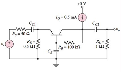
Figure P7.70
(a)
The upper
Answer to Problem 7.70P
Explanation of Solution
Given:
The given circuit is shown below.
The transistor parameters
and
Calculation:
Transconductance
For Input Portion:
Time constant,
For Output portion:
Time constant,
(b)
The small signal mid- band voltage gain
Answer to Problem 7.70P
Explanation of Solution
Given:
The given circuit is shown below.

The transistor parameters
and
Calculation:
Transconductance
(c)
To identify: Whether the upper
Answer to Problem 7.70P
Yes, it is dominated by CL
Explanation of Solution
Given:
The given circuit is shown below.

The transistor parameters
and
Transconductance
Calculation:
For
Time constant,
Upper
Since
Want to see more full solutions like this?
Chapter 7 Solutions
Microelectronics: Circuit Analysis and Design


- Q2. Consider the circuit shown in Figure P7.15. The transistor has parameters B = 120 and VA collector-emitter voltage is VCEO = 1.25 V. (a) Determine Rc, (b) find Ico, and (c) determine the maximum gain. = ∞. The circuit bandwidth is 800 MHz and the quiescent Vcc= 2.5 V RC CL = 0.08 pF Figure P7.15arrow_forwardIn the self-bias circuit of Figure 7.80 a. Draw the transfer characteristic curve of the device. b. Draw additional circuit equations on the same graph. Find c.lDQ and VGSQ. d. Calculate VDS , VD, VG, Vs. ...arrow_forwardQ7. For the PMOS common-source circuit shown in Figure P7.69, the transistor parameters are: VTp = -2 V, K, Cgd = 3 pF. (a) Determine the upper 3 dB frequency. (b) What is the equiv- alent Miller capacitance? State any assumptions or approximations that you make. (c) Find the midband voltage gain. 1 mA/V², 1 = 0, Cgs = 15 pF, and +10 V Rs 0.5 kQ R=8 k2 Ci = 2 µF =Cs=10 µF wwHH R;=0.5 k2 Ce2 2 uF R3 = 22 k23 Rp=D 2 k2 RL= 5 k2 -10 V Figure P7.69 19 WW-arrow_forward
- Problem 7.133(a): For the circuit shown below, let R1 = 106 kN, Rsig = 69 N, and RL Rsig. Assume that %3D 13 kN. Find the value of the bias current I in mA that results in Rin the source provides a small signal vsie and that B = 100. H RL R1 Rsig Ria 8arrow_forward7.65 In the circuit in Figure P7.65, the transistor parameters are: B = 120, VBE(on) = 0.7 V, VA = 100 V, C, = 1 pF, and fr = 600 MHz. (a) Deter- mine C, and the equivalent Miller capacitance CM. State any approxima- tions or assumptions that you make. (b) Find the upper 3 dB frequency and the midband voltage gain. Rc=D4 k2 R = 33 k2 C =1 uF Cc2 = 2 µF Rg = 2 k2 R = 5 ka R2 = 22 k2 Rg%3D 4 k2 Cg = 10 uF Figure P7.65 wwarrow_forward7.65 In the circuit in Figure P7.65, the transistor parameters are: B = 120, VBE(on) = 0.7 V, VA = 100 V, C, = 1 pF, and fr = 600 MHz. (a) Deter- mine C, and the equivalent Miller capacitance Cy. State any approxima- tions or assumptions that you make. (b) Find the upper 3 dB frequency and the midband voltage gain. +5 V Rc-4 k2 R= 33 k2 Ccz =2 AF CCi =1 uF wwwHE Rg = 2 ka 35 k2 R2= 22 ka 4 ks2 ww ww wwarrow_forward
- 7.26. The sampling theorem, as we have derived it, states that a signal x(1) must be sam- pled at a rate greater than its bandwidth (or equivalently, a rate greater than twice its highest frequency). This implies that if x(1) has a spectrum as indicated in Figure P7.26(a) then x(1) must be sampled at a rate greater than 2002. However, since the signal has most of its energy concentrated in a narrow band, it would seem reason- able to expect that a sampling rate lower than twice the highest frequency could be used. A signal whose energy is concentrated in a frequency band is often referred to as a bandpass signal. There are a variety of techniques for sampling such signals, generally referred to as bandpass-sampling techniques. x(t) X(jw) MA @₁ W₂ (a) -W₂ -W₁ p(t) = Σ 8(t-nT) Io. Xp (t) H(jw) 1 -Wo n Wa p(t) H(jw) A+ (b) 3° W wp w x, (t) Figure P7.26arrow_forward7.65 In the circuit in Figure P7.65, the transistor parameters are: B 120, Ver(on)=0.7 V, VA 100 V, C -I pF, and fr mine C, and the equivalent Miller capacitance Cy. State any approxima- tions or assumptions that you make. (b) Find the upper 3 dB frequency and the midband voltage gain. -600 MHz. (a) Deter- +5 V R= 33 ka wwHH Ry=22 k2 4 k2 10 wwarrow_forwardFor the circuit shown below: 1) Calculate the DC bias point for the transistor. 2) Estimate the midband gain with B= 100, Ic = ImA, R= SK2, RL = Ra -SK2, Re - 100KN, VCC = VEE = 10V. 3) With Cet Ca= 47uF and C-47uF, what is the value of the approximate low frequency pole? Ve Re Ce Vaarrow_forward
- A bipolar transistor has parameters B, = 150, C, = 2 pF and C = 0.3 pF and is biased at lco = 0.5 mA. Determine the beta cut-off frequency.arrow_forwardIf the frequency that is injected into an AM modulator is 100Mhz and it is combined with another injected signal of 10Khz, we can say that the combination is:arrow_forwardif the parameters for the BJT given Beta=120, VBE=0.7V, VT=26mV, VA=infinityarrow_forward
 Introductory Circuit Analysis (13th Edition)Electrical EngineeringISBN:9780133923605Author:Robert L. BoylestadPublisher:PEARSON
 Delmar's Standard Textbook Of ElectricityElectrical EngineeringISBN:9781337900348Author:Stephen L. HermanPublisher:Cengage Learning
 Programmable Logic ControllersElectrical EngineeringISBN:9780073373843Author:Frank D. PetruzellaPublisher:McGraw-Hill Education
 Fundamentals of Electric CircuitsElectrical EngineeringISBN:9780078028229Author:Charles K Alexander, Matthew SadikuPublisher:McGraw-Hill Education
 Electric Circuits. (11th Edition)Electrical EngineeringISBN:9780134746968Author:James W. Nilsson, Susan RiedelPublisher:PEARSON
 Engineering ElectromagneticsElectrical EngineeringISBN:9780078028151Author:Hayt, William H. (william Hart), Jr, BUCK, John A.Publisher:Mcgraw-hill Education,