
Concept explainers
Videos
The parameters of the transistors in the circuit in Figure P10.68 are
The currents
Answer to Problem 10.68P
Explanation of Solution
Given:
Calculation:
The given circuit is,
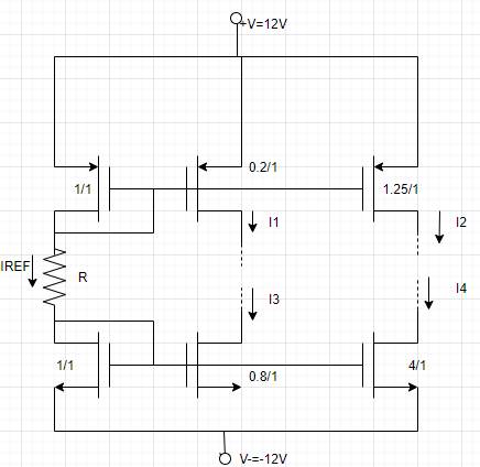
According to the circuit reference current
And
Now substitute the given values in equation (1) and equation (2),
On comparing equation (3) and equation (4),
Now reference current expression is,
Now compare equation (3) and equation (6)
Solve the above expression by quadratic degree method,
Consider
Calculate reference current,
Now calculate current
Conclusion:
Want to see more full solutions like this?
Chapter 10 Solutions
Microelectronics: Circuit Analysis and Design
Additional Engineering Textbook Solutions
Basic Engineering Circuit Analysis
Introductory Circuit Analysis (13th Edition)
Loose Leaf for Engineering Circuit Analysis Format: Loose-leaf
ELECTRICITY FOR TRADES (LOOSELEAF)
Engineering Electromagnetics
ANALYSIS+DESIGN OF LINEAR CIRCUITS(LL)


- Determine the input resistance Rin as indicated in the figure. Ignore resistor ro of the transistor and capacitors are large. A. Rin = R1//R2//R3 B. Rin = R2//R3 (//R4//R5) C. Rin = R2//R3 // ( r π + [1+gm r π ] (//R4//R5) ) D. Rin = R2//R3 // r π (//R4//R5) )arrow_forwardDesign a common-emitter amplifier to provide a small-signal voltage gain of approximately -10. 1. Consider the circuit shown in Figure 1. Show the following calculations in your notebook: Calculate a value for Rc so that A, z –10 Calculate values for R1 and R2 so that the circuit is bias stable and near the center of the load line. (Note: Use the datasheet for the 2N5209 transistor to make your calculations more accurate). Vcc = 10 V R1 Rc Cc2 Cci RL Vs R, REj = 499 Q Figure 1: Common-emitter amplifier for part #1arrow_forwardCoonsider the common emitter amplifier shown in figure below. Assume a β of 100, VBE = 0.7V, VT = 25mA and VA = 100V. Draw an equivalent DC model and determine the rπ, transconductance (gm) and ro. Draw an equaivalent AC model using the small-signal model Find an expression for vbe and vo in terms of the input voltagearrow_forward
- Design counter 0,2,4,6,… with JKFF and DFFarrow_forwardFor the circult shown in the given figure. Rc-2.4 k0, Rg-10 ko. Pmin-50, and Vcc=5 V. Determine the range of values of Vgg 50 Ic that the transistor is in saturation. Assume Vy-0.6 V and VCEsat -0.2 V. The range of values of VB8 Is VBB> 12 V Ra VAR со Va VCE OE RC Nccarrow_forwardUsing LTSpice, simulate the circuit below, use 2N3904 for the transistor. Part ! DC simulation: Measure VCE and Ic. Use .op for the simulation cmd. Remove all capacitors and input signals first. Part 2 AC simulation: Connect all capacitors now and apply an AC signal at the input with an amplitufe of 1mV and a frequency of 1kHz. Determine the Voltage gain of the circuit by dividing Vo with Vin. Show the output for both the DC and AC analysis. Take a screenshot of the circuit and the output voltages and waveforms. Paste in a word file, write your answers, then save as pdf. 50 kΩ Σ 20 0,5 ΚΩ wwwh 9 Vcc=20 V Ca=1 µF = Cc₂ Cg=50 μF 5.6 kn B=100 Ca IST • 3.3 ΚΩ 5 ΚΩΣ CEarrow_forward
- Using the re model circuit, determine the total voltage gain for the BJT circuit shown below. Show the details of your work. 22V ... 5.6k0 330k Vo + 10UF-POL B = 80 1200 10UF-POL To = 40 kN 2N2221 6.8k) Vs 4700 22UF-POLarrow_forwardTime left 1:46:17 A bipolar junction transistor is described in the figure below. The transistor is implemented in the circuit with Vcc, Rc, and RB equal to 16 volts, 2k, and 10kn. Determine the value of Vout if Vin = 1.1V. V... in RB B Vec Ro V E outarrow_forward........ (Figure-1) R. RB= 380kN,Rc= 1kN B = 100, VBB = Vcc=12V RB ww Vec CC ......... I, V CE СЕ V ВЕ BB Q-1-b) Describe briefly the input / output characteristics and application of Common Emitter BJT Configurationarrow_forward
- For the circuit of Figure 2. Carry out the analysis in DC and small signal with www.w www www.www Vt=0.7 V, Kn(W/L) = 4 mA/V. Ignore the Early effect. Determine: (a) The current in DC ID. (b) The gains vo/v₁, io/ii (c) The input resistance Rin and output resistance Rout. wwwwww 06402 www Ca HH {ama Ο ΜΩ www.11 Figura 2: 0.51 k www.li 12 V • 27 ΚΩ Ca +1₁ -0% 4.7 karrow_forward5, a) Determine Vdsat when ID=.5 mA. b) Determine Kn when ID = 0.5 Amps. (Show your work!) c) Determine VTN. (Show your work!) d) Vgs Consider the circuit and corresponding graph, shown below. ID (mA) 0.60 0.50 0.40 0.30 0.20 0.10 0.00 0 0.5 Vds 1 1.5 2 2.5 Vds 3 3.5 4 4.5 5 -Vgs = 1V - Vgs = 1.1V - Vgs = 1.2V - Vgs = 1.3Varrow_forwardFor the circuit given below Given Vsat=12V . I) Identify the stages II) Find the output voltagearrow_forward
 Introductory Circuit Analysis (13th Edition)Electrical EngineeringISBN:9780133923605Author:Robert L. BoylestadPublisher:PEARSON
 Delmar's Standard Textbook Of ElectricityElectrical EngineeringISBN:9781337900348Author:Stephen L. HermanPublisher:Cengage Learning
 Programmable Logic ControllersElectrical EngineeringISBN:9780073373843Author:Frank D. PetruzellaPublisher:McGraw-Hill Education
 Fundamentals of Electric CircuitsElectrical EngineeringISBN:9780078028229Author:Charles K Alexander, Matthew SadikuPublisher:McGraw-Hill Education
 Electric Circuits. (11th Edition)Electrical EngineeringISBN:9780134746968Author:James W. Nilsson, Susan RiedelPublisher:PEARSON
 Engineering ElectromagneticsElectrical EngineeringISBN:9780078028151Author:Hayt, William H. (william Hart), Jr, BUCK, John A.Publisher:Mcgraw-hill Education,