
Videos
Design a bipolar cascode amplifier with a cascode active load similar tothat in Figure P10.89 except the amplifying transistors are to be pnp andthe load transistors are to be npn. Bias the circuit at
The design of a circuit for a given specifications.
To find: The small-signal voltage gain
Answer to Problem D10.90P
The design is shown in Figure 2.
Explanation of Solution
Given:
Calculation:
The given circuit is,
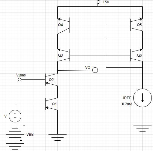
Figure 1
The equivalent designed circuit for active load amplifier is as shown,
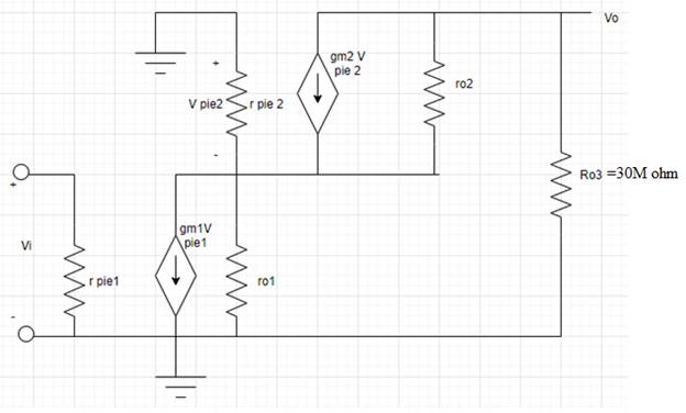
Figure 2
The expression for input voltage
Now expression for output resistance is,
Put equation (3) in equation (2).
Consider
Now expression for hybrid resistor parameter.
Now output voltage will be,
Consider
Put value from equation (8) to equation (6).
Put
Now
Substitute the value for
Now
Substitute the derived values in equation (10).
Want to see more full solutions like this?
Chapter 10 Solutions
Microelectronics: Circuit Analysis and Design


- 2. The circuit in Figure 2 has a BJT transistor with B= 200, VA = 20 V. Determine BJT DC collector current and DC collector voltage. Determine the small-signal input resistance seen by the AC voltage source, the output resistance at Vout, and the transfer function Vout/Vin. HH 1.7 V 100k Figure 2, Problem 2 10 V 2k Vout 2karrow_forwardWith the help of circuit diagrams, list the different biasing methods for D- MOSFET and E-MOSFET amplifiers.arrow_forward(b) The multistage amplifier circuit of Figure Q.2(b) have the following parameters: Qı and Q2: B= 200, VBE = 0.7 V, VT = 26 mV , VA=∞ Given that Icọ1 = 2 mA and VCEQ1 = 2 V. (i) Determine the value for R84. List the assumption/approximation made in the analysis. (ii) Sketch and label the small-signal hybrid-t equivalent circuit at midband frequency range. (iii) Calculate the small signal hybrid-n model parameters: gm and ra for Qı and Then, determine Zi2 and Zo. VSI (iv) Find +15 V TU MA RBI 100 k2 UNIVERSITI { Rc 3.3 k2 RB3 10 kN IcQI Q2 C4 Qi VCEQI Ro TEO ► 50 k2 Rs 100 2 RL V. 10k2 RE 2 kN RB4 C3 Zi2 Z, Figure Q.2(b) AYSIAarrow_forward
- The amplifier circuit below has a single ac input and two ac outputs. Assuming transistor parameters of B= 100 and VBE - 0.6 V: a) Determine the Q point. b) Is the transistor in the active region? Explain thoroughly. c) Construct the T-model of the transistor with all parameters labelled and evaluated. Assume room temperature. d) Draw a complete small signal circuit model, then find the voltage gain for both outputs. e) Based on the analysis results, what is the function of this circuit? Suggest a proper application. 3) Assuming that each output is feeding a 50-k2 resistor, determine the total voltage gain and current gain for both outputs. Also, caleulate the amplifier input resistance and the amplifier output resistances. 10 V 10 V Rc= 3.3 kl 100 kn 8. 50 kn RE = 3 kſ2 3D!arrow_forwardVR2 (t) voltage will be calculated by analyzing the circuit in Figure 2 with a non-linear element using the Small Signal Analysis method. For this purposea) Find the operating point VkQ, IkQ voltage and current values of the nonlinear element.b) Linearize the non-linear element at the operating point.c) Find the voltage VR2 (t) by calculating the effect of the variable source using the linear model.arrow_forwardQ.4/ Refer to the class AB power amplifier shown below:a. Determine the dc parameters VB(Q1), VB(Q2), ICQ, VCEQ(Q1), VCEQ(Q2).b. For the 5Vrms input, determine the power delivered to the load resistor.c. Determine the approximate input resistance seen by the signal source if ac=100arrow_forward
- 2) Consider an enhancement MOSFET common source amplifier circuit in Figure 2(a). The output characteristic is showed in Figure 2(b). Assume that the circuit is operating in the saturation region and k = 5 mA/V2. It also given that ra = ro = 00, Cgd = 2 pF, Cgs = 4 pF, Cas = 1 pF, Cwi = 4 pF and Cwo = 3pF. a. Using DC load line, prove that Ino = 22.5 mA and VpsQ = 5.5 V for Vaso = 2.5V. (Please attach the characteristic graph provided in your working solution) b. Draw the AC equivalent circuit at mid frequency. c. Estimate the voltage gain Av = Vo /Vi. d. Determine the dominant high cut – off frequency for the circuit. 10 V Rp 100 2 6 MQ C2 ci Rs RL Vo 1002 R: 5002 Rs Vo 14 MQ Cs 100 2 Vs Figure 2(a) 60- 50 30 20 10 9. 10 Figure 2(b) (yu) 4arrow_forwardQuestion 2 Referring to Figure 2 and the following BJT parameters: B = 100, thermal voltage = 25 mV and VeE = 0.7 V. If v = (Mx10°)sin(wt) V where M is , 209384 . calculate the instantaneous positive peak collector voltage, Ve(peak). Explain the effect of CE on the BJT DC operating point and the small- signal voltage gain. Vcc 10V Rc $4.7 kN R 47 ko3 HE vo B-100 Vehermar=25mv R. 10 kn R $ika T10UF GND Figure 2arrow_forwardActivity 2: The amplifier circuit below has a single ac input and two ac outputs. Assuming transistor parameters of B= 130 and VBE=0.7 V: 15 V 15 V W 350 ΚΩ 300 ΚΩ H11 13 ΚΩ 10 ΚΩarrow_forward
- 2- Draw a transistor amplifier circuit ( BJT ) Bipolar Junction of type ( NPN ) then write the mathematical relation of Circuit voltage gain factor and what is the factors that depend on and how can we increase the gain factor .arrow_forwardWhat are the advantages of active load with respect to passive load in transistors? Write down at least 5 advantages.arrow_forwardAnswer as correctly as possible, I'll upvote. The MOSFET is designed to be biased on the triode (linear) region. Write the appropriate equation for the small signal voltage gain (vo/vi) as a function of the quiescent point bias voltages VB and VOQ, and the threshold voltage VTH.arrow_forward
 Introductory Circuit Analysis (13th Edition)Electrical EngineeringISBN:9780133923605Author:Robert L. BoylestadPublisher:PEARSON
 Delmar's Standard Textbook Of ElectricityElectrical EngineeringISBN:9781337900348Author:Stephen L. HermanPublisher:Cengage Learning
 Programmable Logic ControllersElectrical EngineeringISBN:9780073373843Author:Frank D. PetruzellaPublisher:McGraw-Hill Education
 Fundamentals of Electric CircuitsElectrical EngineeringISBN:9780078028229Author:Charles K Alexander, Matthew SadikuPublisher:McGraw-Hill Education
 Electric Circuits. (11th Edition)Electrical EngineeringISBN:9780134746968Author:James W. Nilsson, Susan RiedelPublisher:PEARSON
 Engineering ElectromagneticsElectrical EngineeringISBN:9780078028151Author:Hayt, William H. (william Hart), Jr, BUCK, John A.Publisher:Mcgraw-hill Education,