
Videos
The transistor parameters of the circuit in Figure 4.49 are
(a)
The drain current and the individual drain to source voltages of the transistors in NMOS cascade circuit with given transistor parameters.
Answer to Problem 4.12TYU
The quiescent drain current of the transistors are
The drain to source voltage at Q-point for the transistors are
Explanation of Solution
Given Information:
An NMOS cascade device with transistor parameters
Calculation:
Consider the common source amplifier in cascade with a source follower circuit in Figure 1. Here, transistor M1 is operated in common-source configuration and M2 is operated in common-gate configuration.
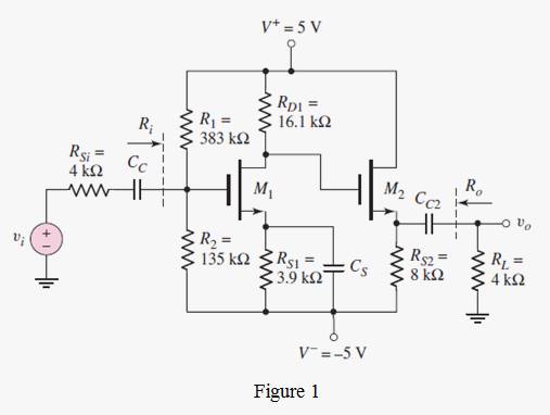
The drain current and gate to source voltage of both the transistors are the same.
The drain current is given by,
The gate to source voltage is given by,
Considering the transistor M1 , the gate voltage for the transistor M1 is,
Substituting the resistance values from the circuit and the bias voltage, the gate voltage is obtained as,
Now, the source voltage is ,
Substituting the resistance value,
Thus, gate source voltage in terms of first transistor is ,
Substituting the expression for gate source voltage in (1), the drain current for transistor M1 in quiescent condition is,
On rearranging the above equation, the final quadratic equation is obtained as
Since the transistor is in saturation, the lower value among the two is considered. Hence, the drain current for the first transistor is,
Now, the drain to source voltage for the transistor M1 can be expressed as,
Substituting the values of parameters,
Considering the transistor M2, the gate voltage is same as the drain voltage of transistor M1, given by
The source voltage is given by,
The gate source voltage is therefore,
The drain current for transistor M2 is given by,
Solving the above expression, the final quadratic equation is obtained as,
Thus, the equation is given by,
Since the transistor is in saturation, the lower value among the two is considered. Hence, the drain current for the second transistor is,
Now, the drain to source voltage for the transistor M2 at Q-point can be expressed as,
Substituting the values of parameters,
(b)
The voltage gain of an NMOS cascade circuit with given transistor parameters.
Answer to Problem 4.12TYU
The voltage gain is given by
Explanation of Solution
Given Information:
:An NMOS cascade device with transistor parameters
Calculation:
Consider the common source amplifier in cascade with a source follower circuit in Figure 1. Here, transistor M1 is operated in common-source configuration and M2 is operated in common-gate configuration.
The voltage gain of the circuit is expressed as,
Here,
Now, the transconductance of the amplifier is given by,
Considering quiescent value of drain current,
Similarly, the transconductance of the second transistor is,
Substituting the transconductance values and the resistor values, the voltage gain is given by,
(c)
The output resistance of an NMOS cascade circuit with given transistor parameters.
Answer to Problem 4.12TYU
The output resistance is given by
Explanation of Solution
Given Information:
An NMOS cascade device with transistor parameters
Calculation:
The output resistance of the circuit is that of the output resistance of the emitter follower circuit which is low. It can be deduced from the small signal equivalent circuit shown below.
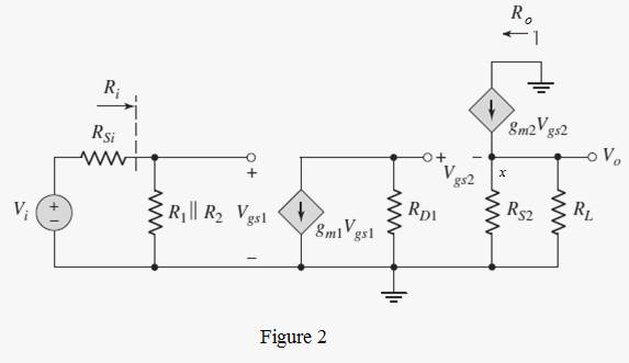
As it appears in the circuit, the output resistance of the circuit excluding the load resistance is obtained by considering the Kirchoff’s current law at the output node x which is,
This implies, the output resistance is given by,
Substituting the resistance and transconductance value,
Want to see more full solutions like this?
Chapter 4 Solutions
Microelectronics: Circuit Analysis and Design


- Solve for Collector Resistance (RC)arrow_forwardA ideal n-channel MOSFET has 525 cm²/V -s parameters = 400 A°. 4. = , Vy = 0.75 V, t When MOSFET is biased in the saturation region at V = 5 V, %3D %3D TN the required rated current is GS I = 6 mA. The required ratio W/L is D( sat)arrow_forwardQ4 VDS=VGS When I = 40 μA, VDs is read as 0.6 V. Increasing I by 50 μA leads to 0.1 V increase in VDs. Find Vand the W/L of the transistor, assume there are no short channel effects.arrow_forward
- The current gain for the transistor in the circuit shown below is B-60, VEn(on) =0.7V and Vic-sat" - 0.2V. For V' = 14.2V when the V, = 3.2V, Rc =8kn and Ic/l =25 find the following: V, Vo Re The value of lc is: O a. 2.188 mA O b. 1.75 mA Oc. 1.4 mA O d. 1.12 mA The value of is Rg: O a. 287.39 kn O b. 229.91 kn O c. 147.14 kn O d. 183.93 kn The value of Vo is: O a. 11.2 V O b.9V O c. 17.5 V O d. 14 Varrow_forwardB: Find the value of RB for the Si transistor circuit as shown in the figure, where the operating point is exactly at the center of the load line, Vcc = 14V, Rc RE = 2KN and B=75. Vcc Rc RB REarrow_forwardQ2 Design a voltage divider bias circuit for an npn silicon transistor having B %D 100 to be used in a Common Emitter configuration. The quiescent point = 1 mA, VCE = 5 V. The supply voltage (Vcc) is 15 V. (Q point) is to be l. Assume VĘ = 0.1Vcc and BRĘ 2 10R2. (a)Find all the resistors values and draw the schematic diagram of this Common Emitter Amplifier with bypass capacitor CE.arrow_forward
- In npn(bipolar junction transistor), the number of charge carriers in the base is more than the emitter. True False . A Moving to another question will save this response.arrow_forwardHow many junctions are in a transistor and how does it “turn on”. What would happen if there were zero resistance (Rc=0) in the collector of a transistor circuit?arrow_forward%3D = 13 volts, Rg = 500 KN, Rc = 6 KN and ß = 120. Assume Transistor is Silicon, VBE=0.7v. For the given circuit, Vcc +Vcc Rc RB VCE V BE a Compute for the base current Q-point, IBq (in Amperes): b. Compute for the collector current Q-point, Ico (in Amperes): c. Compute for the collector-to-emitter voltage, VCEQ (in Volts): d. Draw the DC load line with the axes and the points labeled.arrow_forward
- For the circuit Shown below draw the DC-load line and determine the value of R2 so that the Q-Point located at the current of DC-load line assume β=100arrow_forwardFor the circuit of Figure 2. Carry out the analysis in DC and small signal with www.w www www.www Vt=0.7 V, Kn(W/L) = 4 mA/V. Ignore the Early effect. Determine: (a) The current in DC ID. (b) The gains vo/v₁, io/ii (c) The input resistance Rin and output resistance Rout. wwwwww 06402 www Ca HH {ama Ο ΜΩ www.11 Figura 2: 0.51 k www.li 12 V • 27 ΚΩ Ca +1₁ -0% 4.7 karrow_forward6.39. Assuming perfectly matched transistors, find the approximate values of Ic and VCE in each of tran- sistors Q1. Q2, and Q3 in Figure 6.40. Q+15 V 아+ 10 V 2.5 ka 1.9 mA 6.8 kn 3.2 kn Figure 6.40 (Exercise 6.39)arrow_forward
 Introductory Circuit Analysis (13th Edition)Electrical EngineeringISBN:9780133923605Author:Robert L. BoylestadPublisher:PEARSON
 Delmar's Standard Textbook Of ElectricityElectrical EngineeringISBN:9781337900348Author:Stephen L. HermanPublisher:Cengage Learning
 Programmable Logic ControllersElectrical EngineeringISBN:9780073373843Author:Frank D. PetruzellaPublisher:McGraw-Hill Education
 Fundamentals of Electric CircuitsElectrical EngineeringISBN:9780078028229Author:Charles K Alexander, Matthew SadikuPublisher:McGraw-Hill Education
 Electric Circuits. (11th Edition)Electrical EngineeringISBN:9780134746968Author:James W. Nilsson, Susan RiedelPublisher:PEARSON
 Engineering ElectromagneticsElectrical EngineeringISBN:9780078028151Author:Hayt, William H. (william Hart), Jr, BUCK, John A.Publisher:Mcgraw-hill Education,