
Videos
For the circuit in Figure P4.39,
(a)
The width to length ratio of the transistor in the given circuit.
Answer to Problem 4.40P
The width to length ratio of the transistors is given by
Explanation of Solution
Given Information:
A source follower depletion NMOS circuit with transistor parameters
Calculation:
Consider the given circuit in Figure 1 which consists a source follower depletion NMOS circuit .
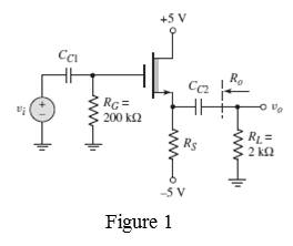
The gate terminal gets grounded when we consider the DC equivalent of the above circuit. The gate current is zero and gate source voltage is expressed as,
The drain to source voltage corresponding to operating point is,
Assuming the transistor is in saturation, the drain current at quiescent condition is given by,
Therefore the above equation can be rearranged to get the W/L ratio as,
Substituting the values of quiescent drain current ,gate-source voltage , threshold voltage and
(b)
The small signal voltage gain for a load resistance.
Answer to Problem 4.40P
The small signal voltage gain for
Explanation of Solution
Given Information:
A source follower depletion NMOS circuit with transistor parameters
Calculation:
For the circuit in Figure 1, the voltage gain is given by,
Here,
Substituting the value of width to length ratio from part (a) along with the voltages and
The transistor output resistance
Substituting these parameters along with the source resistance, the voltage gain can be calculated as,
(c)
The small signal output resistance
Answer to Problem 4.40P
The output voltage is given by
Explanation of Solution
Given Information:
A source follower depletion NMOS circuit with transistor parameters
Calculation:
For the circuit in Figure 1, the small signal output resistance is given by,
The transconductance of the circuit was obtained in previous part as
Substituting these parameters along with the source resistance, small signal output resistance can be calculated as,
(d)
The small signal voltage gain for a load resistance.
Answer to Problem 4.40P
The small signal voltage gain for
Explanation of Solution
Given Information:
A source follower depletion NMOS circuit with transistor parameters
Calculation:
For the circuit in Figure 1, the voltage gain is given by,
The transconductance of the circuit was obtained in previous part as
Now, when there is a finite load resistance which is given here as
Substituting these parameters along with the load resistance resistance, the voltage gain can be calculated as,
It can be observed that, with a finite load resistance, the gain is less compared to the output with infinite load.
Want to see more full solutions like this?
Chapter 4 Solutions
Microelectronics: Circuit Analysis and Design


- Which of the following is a type of Metal Oxide Semiconductor Field Effect Transistor: O P channel JFET O None of them O N channel D- MOSFET in O N channel JFET A simple diode rectifier has 'ripples in the output wave which makes it unsuitable as a DC source. To overcome this one can use of a capacitor in series with a the load resistance. stion Select one: O True O Falsearrow_forward1. For the following circuit assume re = 30.6 1 a. Draw the small signal equivalent circuit. b. Find the input impedance. c. Find output impedance. d. Find the voltage gain. e. Find the current gain. 4.72 10Farrow_forwardQ.3 The input, Vs and the output, Vo of a diode circuit (assuming ideal diode) are shown 3 SEEU/SKEU 1063 in Figure A.2. Name an application that can produce output as in Figure A.2 (ii) and draw the circuit. S UTM S UTM UTM UTM S UTM S UTM O UTM 8 UTM UTM S UTM S UTM UTM UTM S UTM UTM MB UTM ot UTM UT S UTM B UTM UTM 8UTM (i) aUTM UT 8 UTM UTM UTM M UTM TM S UTM UTM UT MS UTM or (i) UTM Figure A.2 8 UTM UT TM S UTMarrow_forward
- A MOSFET operated as a switch as shown in Figure 4.3 permits a digital signal operating at very low current levels to control comparatively high- level current devices such as a light-emitting diode (LED). Analysis a. VG IG VDD b. Repeat for VG = 3.3 V. RD ID ALED VD Figure 4.3: Circuit for Problem 4.3 ermine IG, VD, and ID wh VG = 0 V. The [OSFET is operating region?arrow_forward" A 2N5459 has VGS(off) = -8 v and IDSS = %3D 16mA. What is the drain current at the half cutoff point?arrow_forwardThe negative peak value of output waveform for the given circuit diagram is. (VPP of input is 14 V, Bias voltage is 4 V, Diode is silicon) R: D; VN VouTarrow_forward
- You have been given a Silicon-based BJT transistor with the leads labelled as shown in the figure: Plastic Body TO-92 1. Emitter 2. Base 3. Collector 123 Given that this transistor is either a PNP or NPN variant, create a step-by-step procedure for using a DMM with "diode check" feature to identify whether (a) it's an NPN or PNP (b) it's a PNP or NPN that has failed in some way (e.g. failed as open, or as a short)arrow_forwarde average voltage of Vo. 5 URM U 2 Figure B.2 shows a circuit using two silicon diodes with knee voltage of 0.7 V. The supply voltage, Vs, is a sinusoidal AC signal. The produced output, Vo, is a fluctuating DC signal with ripple peak-to-peak voltage of I.58 V. & UTM UTM UTM STM DI 5 UTM O UTM 50 Hz &UTM UTM UTM 5 UTM UTM UTM 50 µF RL UTM & UTM D2 &UTM/ UTMTUTM (a) Determine the SITM (b) Determine the peak voltage of the Vs. 5 UTM (c) Consider UTM &UTM & UTM waveform of Vo with complete labelling. en Ci is removed from the circuit (i.e. open circuit). Draw the 5 UTM & UTM UTM U1 A TM 5 UTM UTM TM 5 UTM UTMarrow_forward2. In the emitter follower discussed in the lectures, the output (emitter) voltage is 0.7V below the input (base) voltage. One way to remove this offset is to use a diode as shown below left. Suppose our input Vi=2V. Assume beta = 100, VCE,SAT=OV, VBE,ON=0.7, and diode Vş=0.7. +5V +5V 1000 R, 500 1N4148 100 Scattering Limit Vo 10 Vio RL=10 R2 -T,= 25 °C 0.1 1K 0.4 0.8 1.2 1.6 2.0 V, - Forward Voltage (V) 94 9170 a. Determine VB and Vo b. Verify your assumed state of the BJT from (a) c. Verify your assumed state of the diode from (a) d. (Optional challenge) To provide good matching between the diode V; and VBE,ON, we need to have at least 1ma passing through Io, as shown in the datasheet figure above right. What is the maximum V, for which Ip is at least 1mA? To increase this limit, should we change R1 or R2 and in what direction (increase or decrease)? 1,- Forward Current (mA)arrow_forward
- Considering a clamper circuit, where capacitance C, load R, the built-in voltage of diode are unknown, which is the correct statement? The DC level shifts up The DC level of the signal changes The shape of signal changes The peak-to-peak value of signal changesarrow_forwardConsider the following circuit (See image):Show that it is a unity gain absolute value circuit, consider ideal diodesarrow_forwardWhat happens to the depletion width as we increase the doping level on both sides of a p-n junction? Explain conceptuallyarrow_forward
 Introductory Circuit Analysis (13th Edition)Electrical EngineeringISBN:9780133923605Author:Robert L. BoylestadPublisher:PEARSON
 Delmar's Standard Textbook Of ElectricityElectrical EngineeringISBN:9781337900348Author:Stephen L. HermanPublisher:Cengage Learning
 Programmable Logic ControllersElectrical EngineeringISBN:9780073373843Author:Frank D. PetruzellaPublisher:McGraw-Hill Education
 Fundamentals of Electric CircuitsElectrical EngineeringISBN:9780078028229Author:Charles K Alexander, Matthew SadikuPublisher:McGraw-Hill Education
 Electric Circuits. (11th Edition)Electrical EngineeringISBN:9780134746968Author:James W. Nilsson, Susan RiedelPublisher:PEARSON
 Engineering ElectromagneticsElectrical EngineeringISBN:9780078028151Author:Hayt, William H. (william Hart), Jr, BUCK, John A.Publisher:Mcgraw-hill Education,