
(a)
The quiescent values
(a)
Answer to Problem 6.12TYU
The values are
Explanation of Solution
Given:
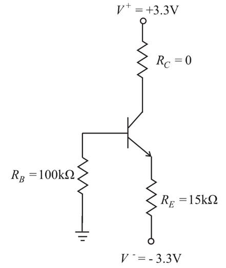
Given circuit:
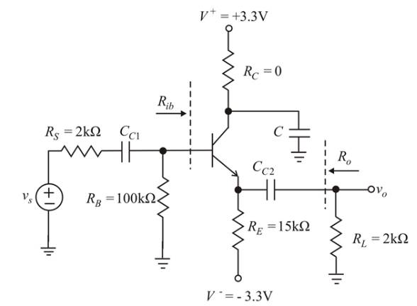
Given Data:
Calculation:
Considering the BJT (Bipolar Junction Transistor) as single node, then, by Kirchhoff's current law, the quiescent emitter current
In CE mode:
The quiescent collector current
Here,
From equations (1) and (2),
(Reducing the ac source
Using equation (3),
From equation (3),
Using equation (4),
Applying Kirchhoff’s voltage law around the collector-emitter loop as,
From equation (2),
Using the equation (4),
(b)
The small-signal voltage gain and small-signal current gain
(b)
Answer to Problem 6.12TYU
The values of small signal voltage and small signal current gain are:
Explanation of Solution
Given:
Given circuit:

Given Data:
Calculation:
Small-signal analysis of given circuit:
[Reducing the dc source to zero and shorting all capacitors]

Determining the Diffusion resistance
Using equation (6),
Let
The input resistance
Using equations (7) and
Let
Using the equation (9),
Finding the Small signal voltage gain
Using equations (7) and
Finding the Small signal current gain
Using equation (9),
(c)
The small-signal input resistance
(c)
Answer to Problem 6.12TYU
The values of small-signal input resistance
Explanation of Solution
Given:
Given circuit:

Given Data:
Calculation:
Small-signal analysis of given circuit:
[Reducing the dc source to zero and shorting all capacitors]
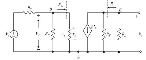
Determining the Diffusion resistance
Using the equation (6),
Let
The input resistance
Using the equations (7) and
Determining the input resistance
From the equation (9), we get
The output resistance
Using the equation (7),
Want to see more full solutions like this?
Chapter 6 Solutions
Microelectronics: Circuit Analysis and Design

- A buck converter is supplied from a 50V battery source. Given L=400uH, C=100uF, R=20 Ohm, f=20KHz and D=0.4. Calculate: (a) output voltage (b) maximum and minimum inductor current, (c) output voltage ripplearrow_forwardFor the circuit shown in Figure 6.17, calculate the following: (a) the frequency of oscillation (b) the value of R3 that will produce the purest sine wave output (c) the value of C that must be connected in series with the 0.08H inductor so that the frequency of oscillation can be made equal to 10kHz RF COIL R2 +Vcc 0.05µF R1 0.08H R3 RCOIL = 1KA re = 250 Q = 8 0.5µF Figure 6.17arrow_forwardExplain what each component is in the design below: DD 7Ro PQ5 8Eo DD 9 So 10 - type of circuit? 1. 6. 2. 7. 3. 8. 4. 9. 5. 10. COarrow_forward
- CBASFEED BUCK 300L 20 桃 1: 200 € 200arrow_forward5) With reference to the circuit diagram given below describe in detail the operation of the circuit diagram with all the applicable waveforms for output voltage, out put current and voltage across the thyristors with alpha=90 degrees Vs = Vo V„ sin wr (a)arrow_forwardProblem-4 a) For the transistor circuit in Figure below, what is VCE When VIN = 0V? (b) What minimum value of Iß is required to saturate this transistor if BDC is 200? Neglect VCE(sat). (c) Calculate the maximum value of RB when VIN = 5 V. RB VINOM Vcc +10 V Rc th 1.0 ΚΩ - VOUTarrow_forward
- Q-4. When VGs of a JFET changes from -3.1 V to -3 V, the drain current changes from 1 mA to 1.3 mA. Then the value of trans-conductance is .arrow_forwardQues-. Full convertor..arrow_forwardAn ideal ac current source is applied to the input terminals of an amplifier, and the amplifier output voltage is 2 V rms. Then, a 2-kΩ resistance is placed in parallel with the current source and the amplifier input terminals, and the output voltage is 1.5 V rms. Determine the input resistance of the amplifier.arrow_forward
- 5) With reference to the circuit diagram given below describe in detail the operation of the circuit diagram with all the applicable waveforms for output voltage, out put current and voltage across the thyristors with alpha=90 degrees Vs = Vm sin wr Vo (a)arrow_forwardDesign a boost converter to provide an output voltage of 36V from a 24V source. The load is 50W. The voltage ripple factor must be less than 0.5%. Specify the duty cycle ratio, switching frequency, inductor and capacitor size, and power devicearrow_forwardb.com Snubbers are an essential part of power electronics to protect the active devices. Design a snubber circuit and explain how thyristors are protected against high di/dt and high dv/dt.arrow_forward
 Introductory Circuit Analysis (13th Edition)Electrical EngineeringISBN:9780133923605Author:Robert L. BoylestadPublisher:PEARSON
 Delmar's Standard Textbook Of ElectricityElectrical EngineeringISBN:9781337900348Author:Stephen L. HermanPublisher:Cengage Learning
 Programmable Logic ControllersElectrical EngineeringISBN:9780073373843Author:Frank D. PetruzellaPublisher:McGraw-Hill Education
 Fundamentals of Electric CircuitsElectrical EngineeringISBN:9780078028229Author:Charles K Alexander, Matthew SadikuPublisher:McGraw-Hill Education
 Electric Circuits. (11th Edition)Electrical EngineeringISBN:9780134746968Author:James W. Nilsson, Susan RiedelPublisher:PEARSON
 Engineering ElectromagneticsElectrical EngineeringISBN:9780078028151Author:Hayt, William H. (william Hart), Jr, BUCK, John A.Publisher:Mcgraw-hill Education,