
Concept explainers
Videos
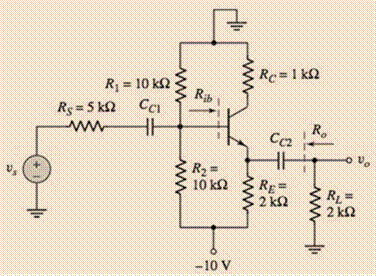
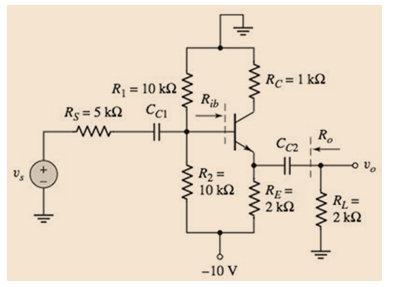
Consider the circuit in Figure P6.45. The transistor parameters are
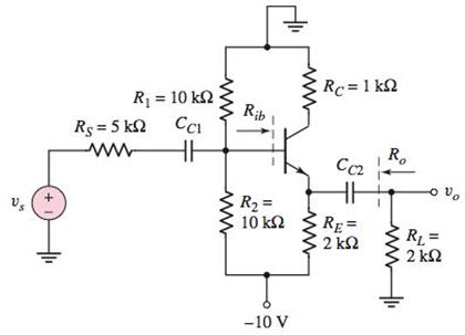
Figure P6.45
a.
The value of the ICQ and VCEQ .
Answer to Problem 6.45P
Explanation of Solution
Given:
The circuit is given as:
Calculation:
Let the BJT be the single node, then by applying Kirchhoff’s current law, the quiescent emitter current
In Common-Emitter mode:
The relation between the quiescent collector current is
For dc analysis,
All the capacitors act as an open circuit and all the ac sources act as short circuits.
DC analysis:
Redrawing the circuit by open circuit, the capacitors, and short circuit the ac sources.
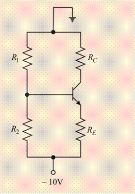
Evaluating the Thevenin resistance
Evaluating the Thevenin voltage,
Drawing the modified circuit:
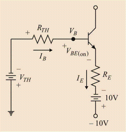
Applying the Kirchhoff s voltage law in the base-emitter loop,
Substituting
From equation (2):
Substituting
Therefore, the value of
From equation (1) and (2):
Substituting
Substitute
Drawing the modified circuit:
Applying Kirchhoff s voltage law to the loop,
Substituting
Therefore, the value of
b.
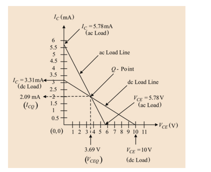
To plot: The dc and the ac load lines.
Explanation of Solution
Given:
The circuit is given as:
Calculation:
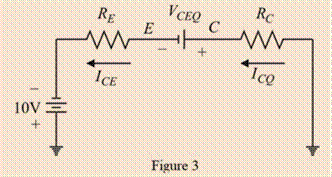
Applying Kirchhoff s voltage law around the collector-emitter loop in figure 1.
Substitute
Substitute
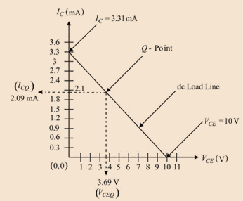
The required “Q” point co-ordinates are
Draw the DC load line:
Drawing the AC equivalent circuit:
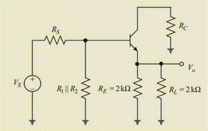
Evaluating the ac load
The expression for the ac load line:
Substitute
Substitute
Drawing the ac load line:
c.
The small signal voltage gain.
Answer to Problem 6.45P
The small signal voltage gain.
Explanation of Solution
Given:
The circuit is given as:
Drawing the small signal analysis of the circuit by short circuiting the dual dc sources and the capacitors:
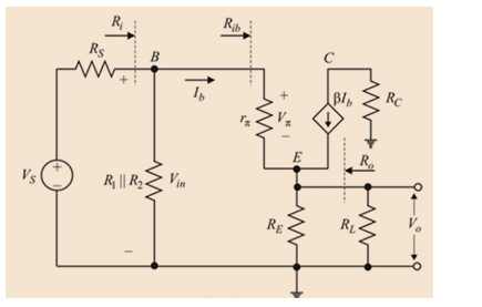
Evaluating the diffusion resistance,
Evaluating the small signal transistor output resistance
Evaluating the input resistance
Calculate the input resistance
The small-signal voltage gain is,
d.
The output resistance.
Answer to Problem 6.45P
The output resistance is
Explanation of Solution
Given:
The circuit is given as
Calculation:
From equation 5,
Thus, the input resistance
Calculate the output resistance,
Therefore, the output resistance
Want to see more full solutions like this?
Chapter 6 Solutions
Microelectronics: Circuit Analysis and Design


- The parameters for each transistor in the circuit shown in Figure P6.75 areβ = 100 and VA = ∞. (a) Determine the small-signal parameters gm , rπ ,and ro for both transistors. (b) Determine the small-signal voltage gainAv1 = vo1/vs, assuming vo1 is connected to an open circuit, and determinethe gain Av2 = vo/vo1. (c) Determine the overall small-signal voltage gainAv = vo/vs. Compare the overall gain with the product Av1 · Av2, using thevalues calculated in part (b)arrow_forwardDraw zener regulator circuit to obtain regulated DC voltage 6.8v . considering input DC voltage in the range from 10v to 30v . consider load resistance of 10kohmarrow_forwardQ6:A) A transistor dissipates 50W in an ambient temperature of 60°C.The thermal resistance are exc-0.5 the junction temperature without a heat sink. Determine the thermal resistance of the heat sink to avoid the junction exceeding 170°C. °CW¹,0a-4°CW.Determine 5% single polver supplyarrow_forward
- All field-effect transistors are unipolar rather than bipolar devices. That is, the main current through them is comprised either of through an N-type semiconductor * ..... .....arrow_forwardIdeally, a dc load line is a straight line drawn on the collector characteristic curves between VCE(cutoff) and /C(sat) the Q-point and cutoff the Q-point and saturation IB = 0 and IB = IC / Bdcarrow_forwardQuestion 6 A large signal circuit model for a MOSFET consists of a dependent current source in parallel with an output resistance, ro, where ro can be expressed as 1/1lp or VA/ID. True Falsearrow_forward
- 5- a-) Define the MOSFET in the figure, explain by drawing its input and output circuit characteristics.b-) Since k=0.1 mA/V2, VGS=5V and VT=2.5V for this MOSFET, find the VDS voltage using the circuit.arrow_forwardCompare hybrid model circuit and re model circuits. Which circuit are you going to recommend in solving AC signal amplifier stage. Defend your answerarrow_forwardMOSFET Amplifier: 1. Determine the drain-to-source voltage (VDs) if VDD = +1sV and RD = 6202. The MOSFET data sheet gives and Ipss = 12 mA. (Ans: Vps=10.6 V) %3Darrow_forward
- draw the following systems: 1- AM generation -Square law product. 2- PM generation- frequency modulator.arrow_forwardCoonsider the common emitter amplifier shown in figure below. Assume a β of 100, VBE = 0.7V, VT = 25mA and VA = 100V. Draw an equivalent DC model and determine the rπ, transconductance (gm) and ro. Draw an equaivalent AC model using the small-signal model Find an expression for vbe and vo in terms of the input voltagearrow_forward(a) Draw the equivalent circuit used for ac analysis of the circuit shown . (Use transistor symbols for this part.) Assume all capacitors have infinitevalue. (b) Redraw the ac equivalent circuit, replacing the transistor with its small-signal model. (c) Identify the function of each capacitor in thecircuit (bypass or coupling).arrow_forward
 Introductory Circuit Analysis (13th Edition)Electrical EngineeringISBN:9780133923605Author:Robert L. BoylestadPublisher:PEARSON
 Delmar's Standard Textbook Of ElectricityElectrical EngineeringISBN:9781337900348Author:Stephen L. HermanPublisher:Cengage Learning
 Programmable Logic ControllersElectrical EngineeringISBN:9780073373843Author:Frank D. PetruzellaPublisher:McGraw-Hill Education
 Fundamentals of Electric CircuitsElectrical EngineeringISBN:9780078028229Author:Charles K Alexander, Matthew SadikuPublisher:McGraw-Hill Education
 Electric Circuits. (11th Edition)Electrical EngineeringISBN:9780134746968Author:James W. Nilsson, Susan RiedelPublisher:PEARSON
 Engineering ElectromagneticsElectrical EngineeringISBN:9780078028151Author:Hayt, William H. (william Hart), Jr, BUCK, John A.Publisher:Mcgraw-hill Education,