
Videos
a.
The value of
a.
Answer to Problem 11.43P
Explanation of Solution
Given:
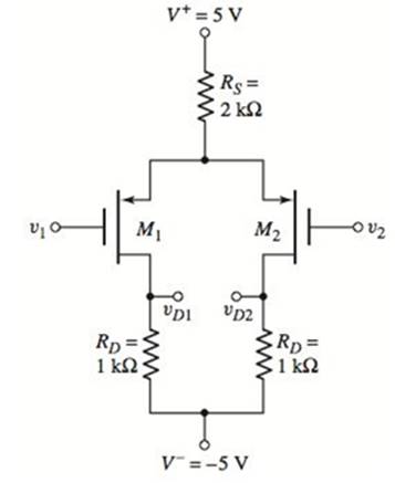
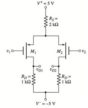
The given circuit is,

Calculation:
Consider the given figure,
Let equate the voltages,
Hence,
b.
The value of
b.
Answer to Problem 11.43P
Explanation of Solution
Given:
The given circuit is,

Calculation:
Consider the given figure,
Let equate the voltages,
Hence,
c.
The value of
c.
Answer to Problem 11.43P
Explanation of Solution
Given:
The given circuit is,
Calculation:
Consider the given figure,
Let equate the voltages,
Hence,
d.
The value of
d.
Answer to Problem 11.43P
Explanation of Solution
Given:
The given circuit is,
Calculation:
Consider the given figure,
Let equate the voltages,
Hence,
Want to see more full solutions like this?
Chapter 11 Solutions
Microelectronics: Circuit Analysis and Design


- The transistor is specified to have Bf in the range of 7 to 35. The load resistance is Rc = 9 ohms. The dc supply voltage is Vcc = 180V and the input voltage to the base circuit is VB = 8V. If VCE (Sat) = 1,1 V and VBE (sat) = 1,6, determine: The value of RB that results in an ODF of 4 A. 0,7514 ohm B 0,5634 ohm C. 0,5081ohm D. 1 ohm The Power loss in the Transistor A. 35,07 W B. 44,30 W c. 40,04 W D. 23,65 Warrow_forwardA base biased transistor circuit with the following element values is given VBB = 10V, VCC = 10V, RB = 470kΩ +/- 5%, RC = 820Ω, β = 100. Find the max and min values of base current. Type your equations and results ..arrow_forwardA modulating signal f(t) has a maximum frequency of 18 kHz and peak value of 3volt, this signal is encoded using PCM. 1- Calculate the number of bits per sample if the number of levels is 130 2- Calculate the SNRQ if the average power of f(t) is 45 watt. 3- Calculate the minimum system bandwidth. e 7:20arrow_forward
- Determine Ic, Ig, lĘ respectively for the PNP transistor shown in the figure below. Assume Is = 5x10-15 A, B = 50, VT= 26mV, VA = ", and Rc = 0.1 KO. %3D 01 Vcc 2V 1.2 V- Rc Select one: Oa. 11.531 mA, 0.231 mA, 11.762 mA b. 5.766 mA, 0.115 mA, 5.881 mA O c 2.306 mA, 0.046 mA, 2.352 mA O d. None of thesearrow_forward19. For the circuit shown in Figure B19a, Va 20V Rc= 3k2 RB = 10k2 VCE Figure B19a Sketch the DC load line in the Graph B19. Calculate the Q point, if the zero signal base current is 50 µA and a =0.991. Mark the Q point in load line. Graph B19 arch (hp 立arrow_forward(b) Draw the ID - VD curves for this MOSFET for ±VD for V₁ = 0 and V₁ = 1 V. VȚ = 1V. n V₁ + p-type D ID V₁arrow_forward
- A (2-2-2) AOI is implemented with transistors allhaving W/L = 2/1. What are the worst-case valuesof τPLH and τPHL if VDD = 2.5 V and C =200 fF?arrow_forward/ Design a circuit using an n-channel E-MOSFET with the following datasheet specifications: Ixon) = 500 mA at VGS 10 V and VGS(h) = 1 V. Use a (+12 V) dc supply voltage with voltage divider bias. The voltage at the drain with respect to ground is to be (+7.78 V), the voltage at the source with respect to the ground is to be (+2.1 V), and the maximum current from the supply is to be 21.1 mA.arrow_forward2) Consider the circuit given below. (Assume: K-4mA/V', Vt=-1V, A=0, (K= µCox.(W/L)) da Perform DC analysis and calculate Va. Vsg, Vs, voltages, and Ip, gm, ro values bo Draw a small-signal equivalent circuit Co Calculate Av, Rin, Rout values as shown on the schematic Also ) satwaton mode Test for Fill inthe table VG VSG O2m A Rin Vs QUin ID vo Coo 9m Ro Av Rout Rin Routarrow_forward
- A MOSFET with k = 4.5 mA/V2 and VT = 3 V is used in the biasing circuit below. Determine the value of VGS. Options: (a) 0 V (b) 3 V (c) 6 V (d) 4.5 Varrow_forwardThe transistor parameters for the differential amplifier shown in Figure P11.32 are VT N = 0.5 V, k n = 80 µA/V2, W/L = 4, and λ = 0. (a) Find RD and IQ such that ID1 = ID2 = 80 µA and vO2 = 2 V when v1 = v2 = 0. (b) Draw the dc load line, and plot the Q-point for M2. (c) What is the maximum common-mode input voltage? Figure p11.32arrow_forwardFor the circuit of Figure 2. Carry out the analysis in DC and small signal with www.w www www.www Vt=0.7 V, Kn(W/L) = 4 mA/V. Ignore the Early effect. Determine: (a) The current in DC ID. (b) The gains vo/v₁, io/ii (c) The input resistance Rin and output resistance Rout. wwwwww 06402 www Ca HH {ama Ο ΜΩ www.11 Figura 2: 0.51 k www.li 12 V • 27 ΚΩ Ca +1₁ -0% 4.7 karrow_forward
 Introductory Circuit Analysis (13th Edition)Electrical EngineeringISBN:9780133923605Author:Robert L. BoylestadPublisher:PEARSON
 Delmar's Standard Textbook Of ElectricityElectrical EngineeringISBN:9781337900348Author:Stephen L. HermanPublisher:Cengage Learning
 Programmable Logic ControllersElectrical EngineeringISBN:9780073373843Author:Frank D. PetruzellaPublisher:McGraw-Hill Education
 Fundamentals of Electric CircuitsElectrical EngineeringISBN:9780078028229Author:Charles K Alexander, Matthew SadikuPublisher:McGraw-Hill Education
 Electric Circuits. (11th Edition)Electrical EngineeringISBN:9780134746968Author:James W. Nilsson, Susan RiedelPublisher:PEARSON
 Engineering ElectromagneticsElectrical EngineeringISBN:9780078028151Author:Hayt, William H. (william Hart), Jr, BUCK, John A.Publisher:Mcgraw-hill Education,