
Concept explainers
Videos
a.
Currents
a.
Answer to Problem 13.10P
Currents
Explanation of Solution
Given:
Circuit is given as;

Current for transistors
For
For
Reference current is given by,
Base to emitter voltage for any transistor is given by,
Therefore base to emitter voltage for transistor
Now, base to emitter voltage for transistor
Now putting the value of equation 2 and equation 3 in equation 1.
Using property of log equation 4 can be written as,
From the given data
Therefore,
Now putting the value of
Therefore reference current is equal to
Now,
Now putting all values,
Base to emitter voltage for transistor
As
Therefore from equation 2 and equation 4.
Now putting all values,
Base to emitter voltage for transistor
As
Therefore from equation 2 and equation 4.
Now putting all values,
b.
Currents
b.
Answer to Problem 13.10P
Currents
Explanation of Solution
Given:
Circuit is given as;
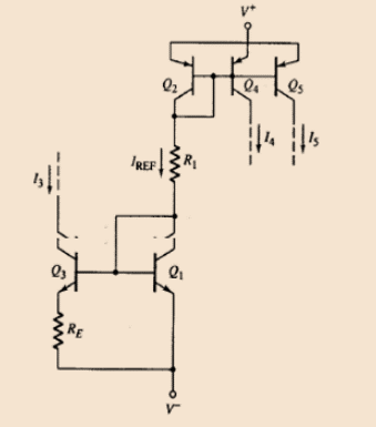
Current for transistors
For
For
Base to emitter voltage for transistor
As
Therefore from equation 2 and equation 4.
Now putting all values,
Base to emitter voltage for transistor
As
Therefore from equation 2 and equation 4.
Now putting all values,
Want to see more full solutions like this?
Chapter 13 Solutions
Microelectronics: Circuit Analysis and Design


- 4. For the transistor in the figure shown below, the parameters are ß = 100 and VÀ = ∞. a. Design the circuit such that lEQ = 1mA and the Q-pt is in the center of the dc load line. b. If the peak-to-peak sinusoidal output voltage is 4V, determine the peak-to-peak sinusoidal signals at the base of the transistor and the peak-to-peak value of Vs. If the load resistor R₁ = 1kQ is connected to the output through a coupling capacitor, determine the peak-to-peak value in the output voltage, assuming vs is equal to the value determined in part (b). Vcc=+10 V www Rs = 0.7 kΩ Cc www RB RE voarrow_forwardQUESTION -3 Calculate the Q point of the given JFET circuit given IDSS =5mA ve VGS(off) = -3.5V. Use mathematical relations (hint: the quadratic relation between current and gate-source voltage). Draw a simple sketch of the VGS – ID plot and show the Q point on this plot. %3D VDD +12 V R1 3.3 M) Rp 1.8 kN R2 2.2 M) Rs 3.3 kNarrow_forwardRe £ Value ZRB 꿀 Consider the transis BE=0.70 The Circuit has the Cirsuit Shown. Let B = 150 Cirbuit shown. and assume that shown .RB below PIRE Rc 47 ки base Current, IB Collector Current, I Mortage 74702 Is V 1201002 the Determine 3. Determine the Determine the Cmitter Vee Determine the value of RB that sets Vce = 0.3 V 2.3 between the Collector andarrow_forward
- ........ (Figure-1) R. RB= 380kN,Rc= 1kN B = 100, VBB = Vcc=12V RB ww Vec CC ......... I, V CE СЕ V ВЕ BB Q-1-b) Describe briefly the input / output characteristics and application of Common Emitter BJT Configurationarrow_forwardHow do you determine when a transistor is in cutoff? A when VE = 0 v B) when VCE = Vcc C) when VCE = Vcc / 2 D when Ic = maximumarrow_forward3. For the circuit on the right, assume that Ic= 1mA, and the transistor is in the active mode (R₁ = Rs = 1k0, B = 100). a- Draw the small signal model and calculate the transistor parameters such as gm and r. b- Calculate the input and output poles of the transistor if C₁ = C₁ = 10:¹2 Farads. H(s) = H nction as Vino Rs S C. R HH₁ RL Cμ Q₁ Vcc Voutarrow_forward
- A MOS transistor acts as voltage dependent current source in Bir MOS transistor . gerilim kontrollü akım kaynağı gibi davranır. Select one: O a. None O b. Triode region (triod bölgesinde) O . Polar region (kutup bölgesinde) O d. Saturation region (doyum bölgesinde) O e. Active region (aktif bölgede)arrow_forwardOpen with v Consider class-A emitter follower circuit shown in the figure below. The circuit parameters are V+ = 24 V, V- = -24 V, and RL = 2000. The transistor parameters are B = 50, VBElon) = 0.7 V, and VCElsat) = 0.2 V. The output voltage is to vary between +20 V and -20 V. The minimum current in Q1 is to be ie1 = 20 mA. For vo = 0, find the power dissipated in the first transistor Q1- V+arrow_forwardFor the emitter-stabilized bias configuration, VCEQ= ---------- if ICQ = 2.4 mA, VCC = 20O V, RC = 470 Q and RE = 2.2 %3D *.kQ 13.592 V O 1113.28 V O -1113.28 V O 18.872 V Oarrow_forward
- What is the output resistance of this circuit in units of ohms? All of the transistors are n-type MOSFETs with kp=0.05 and lambda=0.1. The two DC biasing voltages (Vbias1 and Vbias2) are set to create a current through M3 of 2 mA, current through M2 of 1 mA, and current through M1 of 1 mA. (Hint: Rout is not 10000.)arrow_forwardVcc-+15V RC1 RC2 5 k2 5 ka Vout Vo2 RB1 1 ka RB2 1 ka Q2 Vs2 Vs1 RE 7.5 ka VEE-15V Assume Ql and Q2 are identical transistors with B=hfec=100 and VBE-0.7V. Determine hiej and hiez. Determine the differential gains Ad, (for single-ended) and Ada (for double ended). Determine the common-mode gains Ac, (for single-ended) and Aca (for double ended). Determine the common-mode rejection ratio CMRR for single-ended output. Determine the common-mode rejection ratio CMRR for double-ended output.arrow_forward"It is desirable for the following circuit, assuming the transistors are the same." A) Common fashion gain B) Differential gain mode C) Input resistance network D) CMRR E) What effect does the change in load resistance have on the circuit? Vcc Rc Re Qu, Vi PEE -VEEarrow_forward
 Introductory Circuit Analysis (13th Edition)Electrical EngineeringISBN:9780133923605Author:Robert L. BoylestadPublisher:PEARSON
 Delmar's Standard Textbook Of ElectricityElectrical EngineeringISBN:9781337900348Author:Stephen L. HermanPublisher:Cengage Learning
 Programmable Logic ControllersElectrical EngineeringISBN:9780073373843Author:Frank D. PetruzellaPublisher:McGraw-Hill Education
 Fundamentals of Electric CircuitsElectrical EngineeringISBN:9780078028229Author:Charles K Alexander, Matthew SadikuPublisher:McGraw-Hill Education
 Electric Circuits. (11th Edition)Electrical EngineeringISBN:9780134746968Author:James W. Nilsson, Susan RiedelPublisher:PEARSON
 Engineering ElectromagneticsElectrical EngineeringISBN:9780078028151Author:Hayt, William H. (william Hart), Jr, BUCK, John A.Publisher:Mcgraw-hill Education,