
(a)
The small signal differential-mode voltage gain.
(a)
Answer to Problem 13.5P
The overall small signal differential voltage gain
Explanation of Solution
Given:
The circuit diagram of the BJT op-amp is

Given that
The transistor parameters are,
And base-emitter turn-on voltage is
Calculation:
The differential mode voltage gain can be defined as
Where
From the figure the quiescent collector currents in
Hence,
The collector current for
Therefore, the collector current for
The transconductance can be calculated as
Therefore, the transconductance for
The resistance
Therefore, the resistance
The resistance
Therefore, the resistance
The resistance
Therefore, the resistance
The resistance
Therefore, the resistance
Substitute
Hence,
Substitute
Therefore, the differential mode voltage gain
The small signal voltage gain is

Now,
Therefore,
Where the resistance
Hence,
Equation(2) becomes
Therefore, the small signal voltage gain is
Now the overall small signal differential voltage gain is
Therefore, the overall small signal differential voltage gain
(b)
The differential-mode input resistance.
(b)
Answer to Problem 13.5P
The differential-mode input resistance is
Explanation of Solution
Given:
The circuit diagram of the BJT op-amp is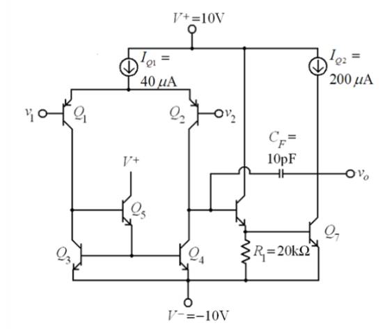
Given that
The transistor parameters are,
And base-emitter turn-on voltage is
Calculation:
The differential-mode input resistance is given as
Where
Hence,
Now, the differential-mode input resistance is
Therefore, the differential-mode input resistance is
(c)
Theunity-gain bandwidth.
(c)
Answer to Problem 13.5P
The gain bandwidth product is
Explanation of Solution
Given:
The circuit diagram of the BJT op-amp is

Given that
The transistor parameters are,
And base-emitter turn-on voltage is
Calculation:
The unity-gain bandwidth product is
Here, the dominant pole frequency is given as
Hence,
And
Hence,
Now the dominant pole frequency we obtain as
Therefore, the dominant pole frequency
The unity-gain bandwidth product is
Therefore, the gain bandwidth product is
Want to see more full solutions like this?
Chapter 13 Solutions
Microelectronics: Circuit Analysis and Design

- A Bipolar junction Transistor with curreat amplification factor being 100, Input Base current is 50μA. Collector voltage is 10 V and biasing voltage being +20 V. Find followings a. Collector current b. Resistance (R1) c. Collector voltage , Emitter voltage , Base Voltage & Collector-Emitter Voltage.arrow_forwardA. Detemine the value of the collector resistor in an npn transistor amplifier with Bpc = 250, VBB = 2.5 V, Vcc = 9 V, VCE = 4 V, and Rg = 100 k2. B. Detemine Ic(sat) for the transistor in below Figure. What is the value of Is necessary to produce saturation? What minimum value of VIN is necessary for saturation? Assume VCE(sat) = 0 V. %3D +5 V 10 kN Rg VINO BDC = 150 1.0 MNarrow_forwardA) Find and draw the equivalent re circuit model. Calculate the voltage gain.arrow_forward
- circuits by using the small signal models of the transistor. Assume the Early voltage of the transistors are infinitely large. Calculate the small-signal input and output impedances of the following Vcc R1 R1 Rout VB RE Rin R2arrow_forwardThe DC Current Gain of a Transistor is Select one: a. Ratio of Collector Current to Base Current b. Ratio of Base Current to Collector Current c. Ratio of Emitter Current to Collector Current d. Ratio of Base Current to Emitter Currentarrow_forwardGiven a D-MOSFET circuit used as an amplifier with the following parameter: IDSS=12mA and a transconductance of gm=3.2 mS. Determine the DC drain to source voltage VDS and the AC output voltage if Vin=500 mV.arrow_forward
- What must be the minimum power rating for the external pass transistor used with a 7815 regulator in a circuit such as that shown in Figure below? The input voltage is 30 V and the load resistance is 10 n. The maximum internal current is to be 700 ma Assume that there is no heat sink for this calculation. Keep in mind that the use of a heat sink increases the effective power rating of the transistor and you can use a lower rated transistor. VIN Re VoUT 7815 RLarrow_forwardIn the circuit given in the figure, Vcc = 15 V, R1 = R2 = 10kΩ, RE = 1KΩ, RL = 0.5kΩ and transistor parameters are given as VBE = 0.7V, ßdc = ß0 = 100. a. Calculate the values of DC bias currents and voltages (IBQ, ICQ and VCEQ). b. Draw the small signal equivalent circuit of the circuit using the hybrid model of the transistor. c. Derive the input impedance expression of the circuit and calculate its value. d. Derive the AVI and AVG voltage gain expressions and calculate their values. e. Derive the current gain expression AI = I0 / Ii and calculate its value. Compare this value you have calculated with the value you will calculate using the expression Aİ = Zi AVI / RL.arrow_forwardThe n-channel enhancement-mode MOSFET of Figure belowarrow_forward
- Diagram show biasing by feedback resistor method.Calculate (i) collector current, and (ii) collector voltage, Given that ß = 100 and transistor is made of sillicon.arrow_forwardExplain Darlington pair circuit with the help of circuit diagram.arrow_forward........ (Figure-1) R. RB= 380kN,Rc= 1kN B = 100, VBB = Vcc=12V RB ww Vec CC ......... I, V CE СЕ V ВЕ BB Q-1-b) Describe briefly the input / output characteristics and application of Common Emitter BJT Configurationarrow_forward
 Introductory Circuit Analysis (13th Edition)Electrical EngineeringISBN:9780133923605Author:Robert L. BoylestadPublisher:PEARSON
 Delmar's Standard Textbook Of ElectricityElectrical EngineeringISBN:9781337900348Author:Stephen L. HermanPublisher:Cengage Learning
 Programmable Logic ControllersElectrical EngineeringISBN:9780073373843Author:Frank D. PetruzellaPublisher:McGraw-Hill Education
 Fundamentals of Electric CircuitsElectrical EngineeringISBN:9780078028229Author:Charles K Alexander, Matthew SadikuPublisher:McGraw-Hill Education
 Electric Circuits. (11th Edition)Electrical EngineeringISBN:9780134746968Author:James W. Nilsson, Susan RiedelPublisher:PEARSON
 Engineering ElectromagneticsElectrical EngineeringISBN:9780078028151Author:Hayt, William H. (william Hart), Jr, BUCK, John A.Publisher:Mcgraw-hill Education,