
Concept explainers
Videos
The output resistance of the 741 op-amp if
Answer to Problem 13.24P
The output resistance is
Explanation of Solution
Given:
Consider the 741 op-amp having bias voltage ±5 V
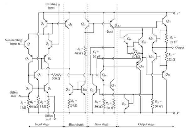
Calculation:
The resistance at
And the output resistance is defined as
Now for solving equation (1) we have
Assuming series resistance of
Where,
And
Where,
The collector current in
The reference current is.
The collector current in
Assuming
And from equation (7),
Now, the current
And the current
Now the resistance
The resistance
Now from the equation (5),
Now from equation (4),
From the equation (3),
Now from the equation (1),
Now from the equation (2),
Want to see more full solutions like this?
Chapter 13 Solutions
Microelectronics: Circuit Analysis and Design


- A 1 - ∅ full-wave rectifier is made by using thyristors. If the peak value of the sinusoidal input voltage is Vm and the value of the delay angle is 45 degree, find the average value of output voltage Select one: a. 0.65 VM b. 0.85 VM c. 0.45 VM d. 0.25 Vmarrow_forwardDraw the waveform of the given clipper circuit and determine the following: a.) At 0V, what is the output voltage?b.) At +20V, what is the output voltage?c.) At -5V, what is the output voltage?arrow_forwardFor the following zener clipper draw the output waveform Vz1 = 5V, Vz1 = 7V VK = 0.8v lkn ISV V₁₂ 5V 2, 72. -5V Q2 Determine The Output Waveform And Calculate The current and PIV 1kQ 1kQ 10 V 10 si www www Q. For the circuit shown in Figure below (1),find the maximum and minimum values of zener diod current. Live 5 ΚΩ www I IL 15 80-120 V 10 ΚΩ LIR 101 102 1015 S Ne 1 k0 www Iz 50 V U2 -ot V. Fumal inasharrow_forward
- A center-tapped FWR circuit have an output dc voltage of 51 V. What is the PIV rating for the diodes? 320.44 V O 160.22 V 80.11 V O 32.47 Varrow_forwardThe DC value of a full-wave rectified voltage with a peak value of 55 V is a.) in bridge-type b.) in center-tappedarrow_forwardUsing an ideal diode, design a clamper circuit that result in the desired output waveform as shown in Figure Q7. Show overall analysis to justify the proposed design. 7. Vo Vi Designed Clamper Circuit - 3 V -20 - 43 V - Fiqure Q7 20arrow_forward
- Show the output voltage for the Vi input voltage in the figure by drawing it along a period (Note: the diode used is a silicon diode, and it won't be considered an ideal diode)arrow_forwardassume that the diodde in the circuit diagram below is reversed, 1.sketch the output waveform (Vo) 2.Determine the DC level of Voarrow_forwardVin What is the steady-state output voltage if diodes. O a. O b. O c. O d. O e. O f. Vin Vo = -34V Vo = -28V vo Vo = -32V Vo = -30V Vo = -36V = 25:1 D2 JFI None 450sin (200t) V? Vy=1V for both Hii D1 VO :2μF =1μFarrow_forward
- Q4) Diode clamps Drive the circuit with a sine wave IK o Vout of 10v amplitude and frequency of Vin 100HZ. Observe the output. What if we change the +5V source to -5V? or even 3V? Explain. +5arrow_forwardThe positive peak value of output waveform for the given circuit diagram is.. . (VPP of input is 14 V, Bias voltage is 4 V, Diode is silicon) R1 I D, VIN VOut VELAS Earrow_forwardFor a silicon BJT shown in figure find Rg that establish VCE = 2 V. Assume VBE = 0.7 V +12V R₂ B 5KQ OC B = 50 Earrow_forward
 Introductory Circuit Analysis (13th Edition)Electrical EngineeringISBN:9780133923605Author:Robert L. BoylestadPublisher:PEARSON
 Delmar's Standard Textbook Of ElectricityElectrical EngineeringISBN:9781337900348Author:Stephen L. HermanPublisher:Cengage Learning
 Programmable Logic ControllersElectrical EngineeringISBN:9780073373843Author:Frank D. PetruzellaPublisher:McGraw-Hill Education
 Fundamentals of Electric CircuitsElectrical EngineeringISBN:9780078028229Author:Charles K Alexander, Matthew SadikuPublisher:McGraw-Hill Education
 Electric Circuits. (11th Edition)Electrical EngineeringISBN:9780134746968Author:James W. Nilsson, Susan RiedelPublisher:PEARSON
 Engineering ElectromagneticsElectrical EngineeringISBN:9780078028151Author:Hayt, William H. (william Hart), Jr, BUCK, John A.Publisher:Mcgraw-hill Education,