
(a)
To find: The quiescent collector currents in transistors.
(a)
Answer to Problem 15.68P
The quiescent collector currents in transistors are
Explanation of Solution
Given:
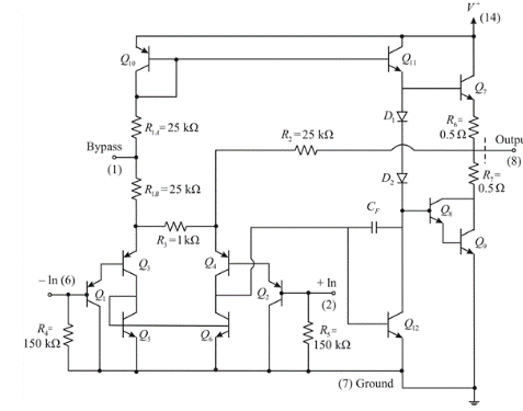
Given LM380 power amplifier circuit as
Calculation:
Assuming matched input transistor and neglecting the base currents. For zero input voltages, the currents in
Since
Hence, the collector current is
Since, the collector currents of
Therefore,
Conclusion:
Therefore, the quiescent collector currents in transistors are
(b)
To find: The quiescent currents inD1, D2, Q7, Q8 and Q9.
(b)
Answer to Problem 15.68P
The quiescent currents are
Explanation of Solution
Given:
Diodes D1 and D2 and transistors Q7, Q8, Q9 are all matched.
Calculation:
The currents in
Hence, the emitter currents of transistor
Therefore, the diode currents are
The voltage across base of
From the circuit given
Thus, the collector current through the transistor
Now, substitute all values in the above expression we have
The base emitter voltages across the transistor
Since,
Taking exponential on both sides,
As the above equation is in the form of polynomial equation, hence the roots are
Thus, the required collector current at transistor
Now, substitute the value of
Thus, the required collector current at transistor
Now, substitute the value of
Thus, the required collector current at transistor
Conclusion:
Thus, the quiescent currents are
(c)
To calculate: The quiescent power dissipated in the amplifier.
(c)
Answer to Problem 15.68P
The required power is
Explanation of Solution
Given LM380 power amplifier circuit as

Calculation:
For no load,
The power dissipated in the amplifier is
Conclusion:
Therefore, the required power is
Want to see more full solutions like this?
Chapter 15 Solutions
Microelectronics: Circuit Analysis and Design

- Qa: A transistor dissipates 50W in an ambient temperature of 60°C, the thermal resistances are 0-0.5 °CW¹, 8ca-4 °CW. Determine the junction temperature without a heat sink. Determine the thermal resistance of the heat sink to avoid the junction temperature exceeding 180°C. )arrow_forward........ (Figure-1) R. RB= 380kN,Rc= 1kN B = 100, VBB = Vcc=12V RB ww Vec CC ......... I, V CE СЕ V ВЕ BB Q-1-b) Describe briefly the input / output characteristics and application of Common Emitter BJT Configurationarrow_forwardThe arrow on the symbol of MOSFET indicates O a. that it is a N-channel MOSFET O b. that it is a P-channel MOSFET Oc. the direction of electrons O d. the direction of conventional current flowarrow_forward
- circuits by using the small signal models of the transistor. Assume the Early voltage of the transistors are infinitely large. Calculate the small-signal input and output impedances of the following Vcc R1 R1 Rout VB RE Rin R2arrow_forwardQues 4: Draw the structure of an N-channel JFET and also explain the drain characteristicsarrow_forwardA circuit responding to temperature is shown in figure 6. Assume the diode equation is given by Ia Ioe(qVa/kT). What is the DC operating point of the circuit at the temperature T. Also determine the small signal output swing Av, due to an incremental change in temperature AT. For this question assume Rį = 0. Heat T+AT V. DD D'B R₁ OV +AV Figure 6: Temperature sensorarrow_forward
- Create a circuit diagram for a half-wave SCR rectifier with an input voltage of 30Vrms, load resistance of 75 ohms, and an SCR firing angle of 45 degrees. Calculate the average output voltage.arrow_forwardQ5(a) Figure Q5(a) shows a basic series voltage regulator circuit. VIN VOUT RREF Q1 U1 R $20 k2 Di R2 30 k2 Figure Q5(a) (i) Calculate the output voltage, VoUT if VIN = 50 V and voltage drop across D, = 6.2 V. (ii) Illustrate a circuit diagram for overload protection between transistor Q1 and the load. (iii) Based on the answer in Q5(a)(ii), calculate the overload current ILmax). (b) Figure Q5(b) shows a voltage regulator. +35 V LM 317 +Vout R1 Vref 220 2 Iref C3 C1 TR2 TADJ C2 R2 5 kn Figure Q5(b) (i) Determine the maximum and minimum output voltage for the voltage regulator in Figure Q5(b), if IADJ = 25 µA and Vref = 0.9 V. (ii) Determine the output voltage of the regulator if R2 is set to 4 kN.arrow_forwardFor the circuit shown in Figure B23, a- 0.97, calculate the following: i. Collector current (Ic) ii. Collector-Base voltage (Ven) i. Emitter Current (I) iv. Base Current (In) Ic 2.5 kl Ouput 2.8V IB 10V Vecarrow_forward
- A 4.7 zener diode is connected to the base resistor. The left side of the resistor sits at about 12V. The right side of the biasing resistor is connected to the Zener and npn transistor. The Zener bias is 5mA. The base current needed is 80uA. What is the appropriate resistor for this circuit? (In kohms) Iarrow_forwardA 4:1 transformer is connected to a bridge rectifier circuit with a lkn load. What is the peak output current of the circuit if the input voltage is 250Vrms? Express your answer in mA.arrow_forwardDesign the transistor shunt regulator to maintain the Vo at a constant value of 12 V. The maximum permissible load current is 460 mA. IC = 12 mA and hFE = 65. The input voltage varies as 20 ± 10%. VBE of the transistor is 0.7 V.arrow_forward
 Introductory Circuit Analysis (13th Edition)Electrical EngineeringISBN:9780133923605Author:Robert L. BoylestadPublisher:PEARSON
 Delmar's Standard Textbook Of ElectricityElectrical EngineeringISBN:9781337900348Author:Stephen L. HermanPublisher:Cengage Learning
 Programmable Logic ControllersElectrical EngineeringISBN:9780073373843Author:Frank D. PetruzellaPublisher:McGraw-Hill Education
 Fundamentals of Electric CircuitsElectrical EngineeringISBN:9780078028229Author:Charles K Alexander, Matthew SadikuPublisher:McGraw-Hill Education
 Electric Circuits. (11th Edition)Electrical EngineeringISBN:9780134746968Author:James W. Nilsson, Susan RiedelPublisher:PEARSON
 Engineering ElectromagneticsElectrical EngineeringISBN:9780078028151Author:Hayt, William H. (william Hart), Jr, BUCK, John A.Publisher:Mcgraw-hill Education,