
Concept explainers
Videos
(a)
The transition points for the p-channel and the n-channel MOSFET.
To sketch: The voltage transfer characteristics.
To find: The value of the input voltage for the different values of the input output voltages.
(a)
Answer to Problem 16.32P
The value of the transition voltages are
Explanation of Solution
Calculation:
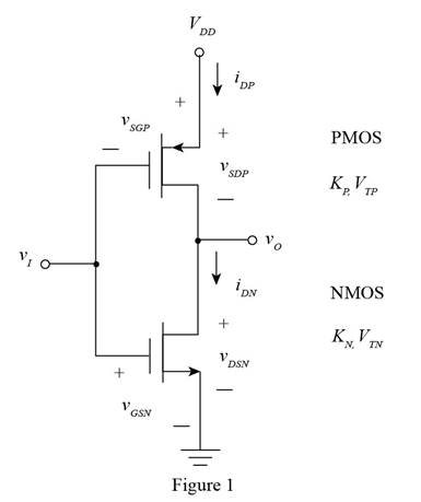
The given diagram is shown in Figure 1
The expression to determine the trans-conductance parameter for NMOS is given by,
Substitute
The expression to determine the trans-conductance parameter for PMOS is given by,
Substitute
The expression to determine the transition points
Substitute
The expression to determine the value of the voltage
Substitute
The expression to determine the value of the voltage
Substitute
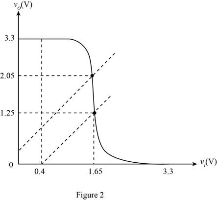
The voltage transfer characteristics is shown below.
The required diagram is shown in Figure 2
The expression to determine the value of the input voltage is given by,
Substitute
The value of the voltage must be less than the supply voltage, thus the input voltage is
The expression to determine the value of the input voltage when the output voltage is more than
Substitute
Conclusion:
Therefore, the value of the transition voltages are
(b)
The transition points for the p-channel and the n-channel MOSFET.
To sketch: The voltage transfer characteristics.
To find: The value of the input voltage for the different values of the input output voltages.
(b)
Answer to Problem 16.32P
The value of the transition voltages are
Explanation of Solution
Calculation:
The expression to determine the trans-conductance parameter for NMOS is given by,
Substitute
The expression to determine the trans-conductance parameter for PMOS is given by,
Substitute
The expression to determine the transition points
Substitute
The expression to determine the value of the voltage
Substitute
The expression to determine the value of the voltage
Substitute
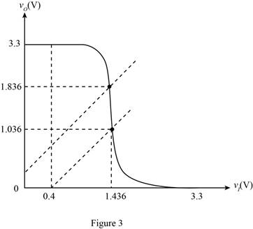
The voltage transfer characteristics is shown below.
The required diagram is shown in Figure 3
The expression to determine the value of the input voltage is given by,
Substitute
The value of the voltage must be less than the supply voltage, thus the input voltage is
The expression to determine the value of the input voltage when the output voltage is more than
Substitute
Conclusion:
Therefore, the value of the transition voltages are
Want to see more full solutions like this?
Chapter 16 Solutions
Microelectronics: Circuit Analysis and Design


- A single phase bridge inverter has an RLC load with R= 20 ohms. L = 32 mH and C = 0.115 mF. The inverter frequency is fo= 60 Hz and DC input voltage is Vs = 110 V. The RMS magnitude of the 1st harmonic of the output current is equal to: Select one: a. 4.34A b. 6.42A OC. 0.955A Qd. None of thesearrow_forwardKit Three: The circuit on the right consists of an inverter connected to a load. Suppose that the range of logical 1 is defined to be 4V to 5V. Determine the restriction, if any, on RL in order that the output be 1 when the input voltage vị is zero. RC R (output)arrow_forwardAn inverter circuit is shown below Vin Voo M₂ •Vout =a) if Vin = 01001110 in what is Vout (11) Draw the wave form of Vin and Vout.arrow_forward
- A single-phase bridge inverter has an RLC load with R20 ohms L-32 mil and C-0115 mF. The inverter frequency is to 60 Hz and DC input voltage is Vs 110 V The phase angle of the load current 5 th harmonics (in degree) is: Select one 0.-28.1 Ob 71.15 ●-71.15 Od 5651 A single phase bridge inverter has an RLC load with R-20 ohm, L32 mit and C-0115 ml The inverter frequency is to 60 Hz and DC input voltage is Vs 110 V The average cument of each transistor is equal to consider up to the fifth hammonies in calculation Select one O None of these OD LEA Oc 223A Od 63A A three phase inverter below has a Y-connected load. The inverter frequency is to 60 Hz and the DC input voltage Vs-220V The applied control signal is a 180 deg conduction mode The RMS Line to Line voltage Vo is equal to Select one O 2425 b. 17963V OC 220N Od. None of thesearrow_forwardV de 2л -а wt a 2л -Vác de An inverter which produces the output voltage shown the figure above is used to supply the series R (=20[Ohm]) and L(330 [mH]) load. Determine the Total Harmonic Distorsion (THD) of the load current up to n 3 for the DC input voltage 125 [V], the output frequency of 60 [Hz], and a=25 [Degree].arrow_forwardThe following circuit represents an NMOS inverter. Calculate the output voltage V for R= 12,604 n, VoD= 5 V, W/L= 4.3, k,= 34 µA/V, Vx =VGs= 4.93 V, and VT= 0 84 V. Note. Your answer should have tow decimal plačes. VDD VDD Voltage levels in the NMOS inverter. V= V OL Rps (a) NMOS NOT gate W sapproximated by Rps= V2s/lp = 1/ K, (Vos – V7) %3Darrow_forward
- a) Find t f, tr , TPLH, TPHL, and tp for the resistively loaded inverter in figure below with C = 0.5 pF and R= 28.8 kN, C=0.5 pF, VDD=5 V, W/L =2.22/1, VH=5 V, VL= 0.20 V, and Ks= (2.22)(100 x 10-6 A/V²). b) Verify your design in part(a) using PSPICE or Multisim package and shows the transient simulation (Time versus Voltage). R 28.8 K VDD 5 V Ms C * 0.5 pF tf t, TPLH, ТРHL, TP Calculated Simulated % Differencearrow_forwardA full bridge inverter with RLC load having the following values: R=7.5 Ohms, L=12.5 mH, C=22 uF. The switching frequency is 500 Hz and the DC input voltage is 180V. The RMS magnitude of the third and fifth harmonics of the load current are respectively equal to: Select one: Oa. 0.3375A, 0.1185A O b. None of these O c. 0.477A, 0.167A d. 0.675A, 0.237Aarrow_forward27 -a wt a π-α π 2л -Vá An inverter which produces the output voltage shown the figure above is used to supply the series R (=10[Ohm]) and L(=20 [mH]) load. Determine the value of a to produce an output with an amplitude of 25 V at the fundamental frequency for the DC input voltage 125 [V] and the output frequency of 60 [Hz].arrow_forward
- a) Design a saturated load inverter shown in the figure below with VDD = 3.3 V and VL = 0.25 V. Assume Ipp = 30 µA, K’n = 25 µA/V²' and VIN = 0.65 V. Verify your design using PSPICE or Multisim package. b) Find the noise margins (NML and NMH) associated with the designed inverter graphically and compare them with your calculation. VDD ML HE VSB Msarrow_forward1. Five identical inverters are connected in a chain. The low-to-high propagation delay of the inverter is 12ns while the high-to-ow propagation delay is 10ns. The input at the first inverter is changed from 1 to 0 at time t-Ons. How long will it take before the output of the 5th inverter change from 0 to 1? Select one: a. 60 ns b. 54 ns. c. 56 ns d. 50 ns. 2. Which of the following statements is/are TRUE? (Choose all that apply) Select one or more: a. The noise margin of a gate indicates the amount of noise it adds to system. b. Glitches always occur when there is unbalanced delays in inputs of gates. c. The propagation delay of a gate varies with its actual fan-out. d. The propagation delay of gates within a digital system affects the maximum frequency that the system can operate.arrow_forwardFor designing a circuit which adds two 10-bit numbers and then complements the sum, which of the following combination of components may be used? O a. 10 half adders and 10 inverters. O b. 10 full adders and 10 inverters. O c. 5 full adders and 5 inverters. O d. 10 half adders and 5 inverters. Windows buiarrow_forward
 Introductory Circuit Analysis (13th Edition)Electrical EngineeringISBN:9780133923605Author:Robert L. BoylestadPublisher:PEARSON
 Delmar's Standard Textbook Of ElectricityElectrical EngineeringISBN:9781337900348Author:Stephen L. HermanPublisher:Cengage Learning
 Programmable Logic ControllersElectrical EngineeringISBN:9780073373843Author:Frank D. PetruzellaPublisher:McGraw-Hill Education
 Fundamentals of Electric CircuitsElectrical EngineeringISBN:9780078028229Author:Charles K Alexander, Matthew SadikuPublisher:McGraw-Hill Education
 Electric Circuits. (11th Edition)Electrical EngineeringISBN:9780134746968Author:James W. Nilsson, Susan RiedelPublisher:PEARSON
 Engineering ElectromagneticsElectrical EngineeringISBN:9780078028151Author:Hayt, William H. (william Hart), Jr, BUCK, John A.Publisher:Mcgraw-hill Education,