
Concept explainers
Videos
To plot: The graphof
To find: The value of
Answer to Problem 16.79P
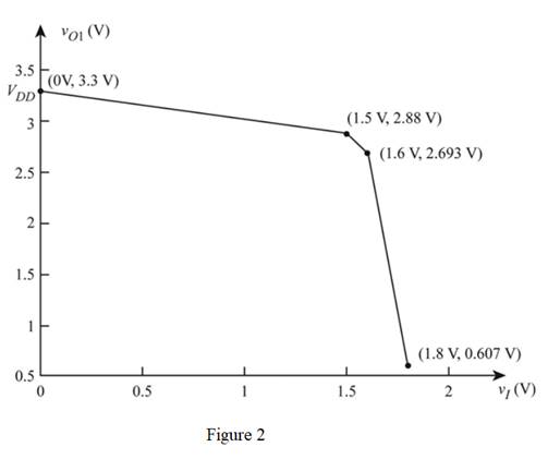
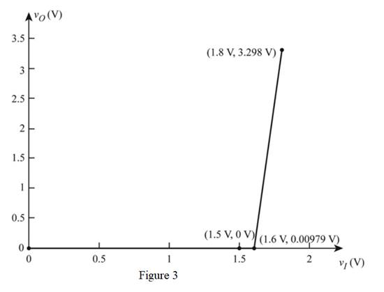
The required plots are shown in Figure 2 and Figure 3. The value of the voltage
Explanation of Solution
Given:
The given diagram is shown in Figure 1.
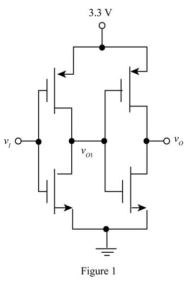
Calculation:
The expression to determine the transition points
Substitute
Case(i)
The expression to determine the output voltage of the first CMOS inverter is given by,
Substitute
The expression to determine the output voltage of the second CMOS inverter is given by,
Substitute
Thus the value of the of appropriate voltage is
Case (ii)
The expression to determine the output voltage of the first CMOS inverter is given by,
Substitute
The bias voltage is
The expression to determine the output voltage of the second CMOS inverter is given by,
Substitute
Thus the value of the of appropriate voltage is
Case (iii)
The expression to determine the output voltage of the first CMOS inverter is given by,
Substitute
The bias voltage is
The expression to determine the output voltage of the second CMOS inverter is given by,
Substitute
Thus the value of the of appropriate voltage is
Case (iv)
The output voltage of the first and the second CMOS inverter is switching point when the input voltage is the
The plot for the voltage between
The plot between the second CMOS inviter output
The required plot is shown in Figure 3
Conclusion:
Therefore, the required plots are shown in Figure 2 and Figure 3. The value of the voltage
Want to see more full solutions like this?
Chapter 16 Solutions
Microelectronics: Circuit Analysis and Design


- A single phase bridge inverter has an RLC load with R= 20 ohms, L= 32 mH and C= 0.115 mF. The inverter frequency is fo= 60 Hz and DC input voltage is Vs 110 V. If the peak magnitudes of the output current and its fundamental are equal to 6.3A and 6.14A, then the power absorbed by the load Po and the fundamental power Po1 are equal to: Select one: O a. 397.56W and 377W b. 795.12W and 754W O c. 562.23W and 533.16W Od. None of thesearrow_forward27 -a wt a π-α π 2л -Vá An inverter which produces the output voltage shown the figure above is used to supply the series R (=10[Ohm]) and L(=20 [mH]) load. Determine the value of a to produce an output with an amplitude of 25 V at the fundamental frequency for the DC input voltage 125 [V] and the output frequency of 60 [Hz].arrow_forwardA single phase bridge inverter has an RLC load with R= 20 ohms. L = 32 mH and C = 0.115 mF. The inverter frequency is fo= 60 Hz and DC input voltage is Vs = 110 V. The RMS magnitude of the 1st harmonic of the output current is equal to: Select one: a. 4.34A b. 6.42A OC. 0.955A Qd. None of thesearrow_forward
- The following circuit represents an NMOS inverter. Calculate the output voltage V for R= 12,604 n, VoD= 5 V, W/L= 4.3, k,= 34 µA/V, Vx =VGs= 4.93 V, and VT= 0 84 V. Note. Your answer should have tow decimal plačes. VDD VDD Voltage levels in the NMOS inverter. V= V OL Rps (a) NMOS NOT gate W sapproximated by Rps= V2s/lp = 1/ K, (Vos – V7) %3Darrow_forwardV DD V DD Figure 3 d M6 M2 CLK –|M4 CLK - |Mg D CLK –|M3 CLK H|M, Qs M1 M5 (c) Figure 3 shows the master and slave latch with an inverter in between. For the data input D and the clock signal CLK, draw the corresponding outputs Qm and Qs. Assume that CLK and CLK have an overlap. 0.4 0.2 timelsec) in)arrow_forwardProblem 2: For the following circuit shown below, what is the function F that the circuit corresponds to ? F = A DrF Convert the circuit above to a NAND + INVERTER implementation in mixed- logic notation. You may use the circuit below for rough work and show your final Oplementation in the last box below. Make sure you cancel bubble pairs, eta . A FINAL MIXED LOGIC NAND-INV IMPLEMENTATION Aarrow_forward
- The duty cycles for 3rd harmonic injection PWM is given by: ki sin(wt)+k2 sin(3wt) da 2 ki sin (wt-)+ką sin(3wt) de ki sin(wt- )+k2 sin(3wt) + 3 do 2 Derive the numeric value of coefficient k1 and k2 to get maximum voltage at the inverterarrow_forwardConsider a CMOS inverter, which the following device parameter nMOS VTO, n = 0.8 V pMOS VTO, p = -1.0V unCox = 50 μA/V² upCox = 20 μA/V² The power supply voltage is VDD = 5V. Both transistors have a channel length of Ln = Lp = 1 um. The total output load capacitance of this circuit is Cout= 2 pF, which is independent of transistors dimensions. i) ii) iii) Determine the channel width of the nMOS and the pMOS transistors such that the switching threshold voltage is equal to 2.2 V, and the output rise time is Trise = 5 ns Calculate the average propagration delay time tp for the circuit designed in (a) How do the switching threshold Vth and the delay times change if the power supply voltage is dropped from 5 V to 3.3 V. Provide the interpretation of the results.arrow_forwardA full bridge inverter with RLC load having the following values: R=7.5 Ohms, L=12.5 mH, C-22 uF. The switching frequency is 500 Hz and the DC input voltage is 180V. The average current supply (consider up to the fifth harmonics in calculation) would be equal to: Select one: a. None of these b. 3.84A Ⓒc. 1.64A Ⓒd. 5.74Aarrow_forward
- A CMOS inverter is to be designed to hate mid-point voltage V₁ equal to half of Vdd- Given the following parameters: µµCox=100 µA/V² ; VÊ-0.7 V for NMOS µpCox=40 µA/V² ; Vtp=-0.9 V for PMOS Find the ratio of (W/L)n to (W/L)p.arrow_forwarda) Design a saturated load inverter shown in the figure below with VDD = 3.3 V and VL = 0.25 V. Assume Ipp = 30 µA, K’n = 25 µA/V²' and VIN = 0.65 V. Verify your design using PSPICE or Multisim package. b) Find the noise margins (NML and NMH) associated with the designed inverter graphically and compare them with your calculation. VDD ML HE VSB Msarrow_forwardi) Construct a CMOS NAND gate, NMOS NAND gate and NMOS NOR gate. ii) What are the differences between Resistor Transistor Logic, Directly Coupled Transistor Logic and Transistor Transistor Logic? Draw 3 input NAND using RTL, 4 input NAND using DCTL. iii) A certain gate draws 3mA when its output is HIGH and its average power dissipation, Vcc is 7V for Transistor Transistor Logic. How much does the gate draw when its output is LOW? It draws 4.5 mA when in Transition time. Determine average power dissipation for CMOS. iv) Determine if the LSTTL (5V) can drive a CMOS (5V, HCT) circuit and vice ve sa. Voh Vol Vih Vil LSTTL 2.8 0.38 1.9 0.9 CMOS 2.3 0.75 2.85 0.75arrow_forward
 Introductory Circuit Analysis (13th Edition)Electrical EngineeringISBN:9780133923605Author:Robert L. BoylestadPublisher:PEARSON
 Delmar's Standard Textbook Of ElectricityElectrical EngineeringISBN:9781337900348Author:Stephen L. HermanPublisher:Cengage Learning
 Programmable Logic ControllersElectrical EngineeringISBN:9780073373843Author:Frank D. PetruzellaPublisher:McGraw-Hill Education
 Fundamentals of Electric CircuitsElectrical EngineeringISBN:9780078028229Author:Charles K Alexander, Matthew SadikuPublisher:McGraw-Hill Education
 Electric Circuits. (11th Edition)Electrical EngineeringISBN:9780134746968Author:James W. Nilsson, Susan RiedelPublisher:PEARSON
 Engineering ElectromagneticsElectrical EngineeringISBN:9780078028151Author:Hayt, William H. (william Hart), Jr, BUCK, John A.Publisher:Mcgraw-hill Education,