
Concept explainers
Videos
(a)
The value of the input switching voltage and the input voltage for the given
(a)
Answer to Problem 16.33P
The value of the input switching voltage is
Explanation of Solution
Calculation:
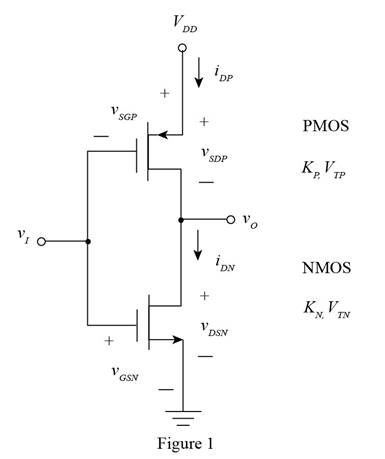
The given diagram is shown in Figure 1
The expression to determine the trans-conductance parameter for NMOS is given by,
Substitute
The expression to determine the trans-conductance parameter for PMOS is given by,
Substitute
The expression to determine the transition points
Substitute
The expression to determine the value of the input voltage is given by,
Substitute
The expression to determine the value of the input voltage when the output voltage is more than
Substitute
Conclusion:
Therefore, the value of the input switching voltage is
(b)
The value of the input switching voltage and the input voltage for the given
(b)
Answer to Problem 16.33P
The value of the input switching voltage is
Explanation of Solution
Calculation:
The expression to determine the trans-conductance parameter for NMOS is given by,
Substitute
The expression to determine the trans-conductance parameter for PMOS is given by,
Substitute
The expression to determine the transition points
Substitute
The expression to determine the value of the input voltage is given by,
Substitute
The expression to determine the value of the input voltage when the output voltage is more than
Substitute
Conclusion:
Therefore, the value of the input switching voltage is
Want to see more full solutions like this?
Chapter 16 Solutions
Microelectronics: Circuit Analysis and Design


- A single phase bridge inverter has an RLC load with R= 20 ohms. L = 32 mH and C = 0.115 mF. The inverter frequency is fo= 60 Hz and DC input voltage is Vs = 110 V. The RMS magnitude of the 1st harmonic of the output current is equal to: Select one: a. 4.34A b. 6.42A OC. 0.955A Qd. None of thesearrow_forwardA full bridge inverter with RLC load having the following values: R=7.5 Ohms, L=12.5 mH, C-22 uF. The switching frequency is 500 Hz and the DC input voltage is 180V. The average current supply (consider up to the fifth harmonics in calculation) would be equal to: Select one: a. None of these b. 3.84A Ⓒc. 1.64A Ⓒd. 5.74Aarrow_forwardAn inverter circuit is shown below Vin Voo M₂ •Vout =a) if Vin = 01001110 in what is Vout (11) Draw the wave form of Vin and Vout.arrow_forward
- The duty cycles for 3rd harmonic injection PWM is given by: ki sin(wt)+k2 sin(3wt) da 2 ki sin (wt-)+ką sin(3wt) de ki sin(wt- )+k2 sin(3wt) + 3 do 2 Derive the numeric value of coefficient k1 and k2 to get maximum voltage at the inverterarrow_forward4. A CMOS inverter has Vtp = -0.6 V, (W/L), = 6, and Kp = HpEox/2Tox = 28 µA/V², and %3D %3D %3D CL = 25 fF. Calculate the rise time delay for a) VDD = 2.5 V, b) VDD = 1.8 V.arrow_forwardParallel resonant inverters are mostly known for the following features: Select one: O a. None of these O b. The output current is dependent from the load. O c. The resonant circuit, load and switch are all in parallels O d. It has the advantage of requiring small reactive components Consider a full-bridge resonant inverter. The switching sequence of the devices is Select one: O a. Q1D1, Q2D1, Q3D4, Q4D3 O b. Q1D1, Q2D2, Q3D3, Q4D4 O c. Q1Q2, D3D4, Q3Q4, D1D2 O d. Q1Q2, D1D2, Q3Q4, D3D4 The gating technique using a train of pulses is suitable for: Select one: O a. Resistive and inductive loads O b. Resistive loads O c. Inductive loads O d. None of thesearrow_forward
- 4. Consider the circuit below on the left. a) What logic function does it perform? (What is F in terms of inputs A and B?) b) Find the transistor sizes (NMOS and PMOS widths) so that the fundamental dynamics are that of the symmetrical inverter on the right. VDD Ā- A - B 6W F 3W A Вarrow_forwardAn inverter with a resistive load, VDD = 3.3 V, P = 0.1 mW, VL = 0.2 V, K'n = 60 UA/V2 and VT N = 0.75 V. The value of (W/L)S is:arrow_forwardV de 2л -а wt a 2л -Vác de An inverter which produces the output voltage shown the figure above is used to supply the series R (=20[Ohm]) and L(330 [mH]) load. Determine the Total Harmonic Distorsion (THD) of the load current up to n 3 for the DC input voltage 125 [V], the output frequency of 60 [Hz], and a=25 [Degree].arrow_forward
- 2-a *-a R 27 limini An inverter which produces the output voltage shown the figure above is used to supply the series R (-10[Ohm]) and L(-20 [mH]) load. Determine the value of a to produce an output with an amplitude of 10 V at the fundamental frequency for the DC input voltage 200 [V] and the output frequency of 60 (Hz).arrow_forwardKit Three: The circuit on the right consists of an inverter connected to a load. Suppose that the range of logical 1 is defined to be 4V to 5V. Determine the restriction, if any, on RL in order that the output be 1 when the input voltage vị is zero. RC R (output)arrow_forwardConsider the oscillator circuit. If we had 9 inverters with identical toreland teu, values, what would the oscillation frequency be? If we had 8 inverters, what would the oscillation frequency be? VDD VDD VDD C2 C3 0.1µF 0.1µF 0.1μFarrow_forward
 Introductory Circuit Analysis (13th Edition)Electrical EngineeringISBN:9780133923605Author:Robert L. BoylestadPublisher:PEARSON
 Delmar's Standard Textbook Of ElectricityElectrical EngineeringISBN:9781337900348Author:Stephen L. HermanPublisher:Cengage Learning
 Programmable Logic ControllersElectrical EngineeringISBN:9780073373843Author:Frank D. PetruzellaPublisher:McGraw-Hill Education
 Fundamentals of Electric CircuitsElectrical EngineeringISBN:9780078028229Author:Charles K Alexander, Matthew SadikuPublisher:McGraw-Hill Education
 Electric Circuits. (11th Edition)Electrical EngineeringISBN:9780134746968Author:James W. Nilsson, Susan RiedelPublisher:PEARSON
 Engineering ElectromagneticsElectrical EngineeringISBN:9780078028151Author:Hayt, William H. (william Hart), Jr, BUCK, John A.Publisher:Mcgraw-hill Education,