
Videos
An integrator with input and output voltages that are zero at
(a)
The value of the output voltage for different time interval.
Answer to Problem 9.9EP
Thevalue of the output voltage for the different time interval is
Explanation of Solution
Calculation:
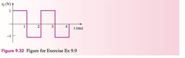
The given diagram is shown in Figure 1
From the above waveform the expression for the voltage is given by,
Mark the values and draw the integrated op-amp circuit.
The required diagram is shown in Figure 2
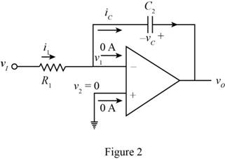
Apply KVL at the feedback loop.
Substitute
The conversion from
The conversion from
The conversion from
The conversion from
The conversion from
The conversion from
The conversion from
The conversion from
Apply KCL at the inverting terminal.
Substitute
Substitute
The expression for the output voltage for the time
Substitute
The expression for the output voltage for the time
The expression for the output voltage for the time
Substitute
The expression for the output voltage for the time
The value of the voltage output voltage for different time interval is given by,
Conclusion:
Therefore, the value of the output voltage for the different time interval is
(b)
The value of the output voltage for different time interval.
Answer to Problem 9.9EP
Thevalue of the output voltage for the different time interval is
Explanation of Solution
Calculation:
The expression for the output voltage for the time
Substitute
The expression for the output voltage for the time
The expression for the output voltage for the time
Substitute
The expression for the output voltage for the time
The value of the voltage output voltage for different time interval is given by,
Conclusion:
Therefore, the value of the output voltage for the different time interval is
Want to see more full solutions like this?
Chapter 9 Solutions
Microelectronics: Circuit Analysis and Design


- Graphically show the output voltage (Vo) and load current (IL) by simulating the difference receiving Op-Amp circuit given in the figure.(PSIM using PSpice or)R1 = R2=10kΩRL=1.5 kΩRf=14kΩarrow_forward3. The input voltage of the following differentiator op-amp circuit is given; sketch the output voltage waveform of the circuit. Vin 0.01 μF R₁ M 100KQ2 +12V -12V M outarrow_forwardI designed a summing amplifier that could amplify a 1mV sinusoid (Vina) into a sinusoid with 1V amplitude and 3.5V offset. The value for R1a is 1k ohms, for R1b is 1mega ohms, R2 is 1 mega ohms, and Vin b is -3.5V. What is the input offset voltage?arrow_forward
- (IV) A specialist sensor is being used to detect the pollution being emitted from an engine. The true signal is in the range of 30-50mV DC but is being affected by 800HZ AC noise from the electronic engine controller. Design a modular system consisting of a filter (that removes the noise) and an op-amp based amplifier (that increases the signal to a range of 3-5V DC) (V) The op-amp used in part (iv) above has an open-loop (i.e. without feedback) gain-frequency graph as shown below. 100000 10000 1000 100 10 1 10 100 1000 10000 100000 1000000 10000000 Frequency (H2) Voltage Gain, Av (Vout/Vin)arrow_forwardQuestion 1: a) Sketch Vo versus time for the circuit shown with the input given. b) Determine DC output voltage without a capacitor. c) If a capacitor of 10 uF is placed in parallel with RL, sketch the vo versus time. d) find the DC output voltage. Given R1 = R2 = RL = 2.2 k2. Vi +40 D1. D2 10 ms R = 2.2 k2 ww R%3D 1GF R = -40 2.2 k2 2.2 k2arrow_forwardIn the circuit in the figure Vcc= 25 V, Vi= 40 mV, RB = 470 kg. RC = 3.3 kg, RE1 = 470 G, RE2 = 1.2 kg RL = 32.5 k(2 and B = 110 because you find the value of the output voltage (Vo) according to. Note-1: capacitors are worth neglecting at mid-band frequency. Note-2: the output impedance (ro) of the transistor will be ignored. RB Q1 NPN RCarrow_forwardIn Figure is given . Ri(s). R:() R() Y(s) 22 - G(s) O A) multiple input and single output system (MISO) O B) there are not correct answers C) single input and single output system (SISO) O D) single input and multiple output system (SIMO) E) multiple input and multiple output system (MIMO)arrow_forwardWhich of the following are most true when comparing balanced (differential) signals to unbalanced (single-ended) signals?A. Balanced signals are less susceptible to noise interference.B. Unbalanced signals use fewer wires.C. Balanced signals use ground for one of the two wires.D. Unbalanced signals take advantage of the common-mode rejection capability of op amps.Two correct possible answers.arrow_forwardDraw the necessary waveforms. non - Inverting op-amp Rr +10V Ri Vo 3 741 V;=1V -10V 500HZ GNDarrow_forwardVi is a sinusoid signal of 8 Vp-p and f = 1 kHz. Vref = 2 V and V1 = 5 V and V2 = -1V. Assume that V1 is connected to pin7 of op-amp 741 and V2 is connected to pin 4. The output Vo will be, * V1 Vo 741 Vret O A square wave of 6 Vp-p, 1 kHz A rectangular wave of 6 Vp-p, 1 kHz A triangular wave of 6 Vp-p, 1 kHz A sinusoid wave of 8 Vp-p, 1 kHz A rectangular wave of 4 Vp-p, 1 kHz A square wave of 8 Vp-p, 1 kHz A sawtooth wave of 6 Vp-p, 1 kHz O A sinusoid wave of 6 Vp-p, 1 kHzarrow_forwardDesign a mutivibrator circuit to give the output waveform below? Use any necessary assumption you want. (Time in millisecond) 2 2 6arrow_forwardAn op-amp comparator in a firing circuit can produce waveforms at the output of up to 28 V peak-to-peak without any distortion. An inverse cosine-based firing circuit with a voltage range from +14 to -14 (reference voltage) is used to produce a gating signal for the SCR at the desired delay angle. if the desired firing angle is 120 degrees, the reference voltage must be: O A. 12 O B. -7 O C. None of the other choices are correct O D.-12 O E. 7arrow_forwardarrow_back_iosSEE MORE QUESTIONSarrow_forward_ios
 Introductory Circuit Analysis (13th Edition)Electrical EngineeringISBN:9780133923605Author:Robert L. BoylestadPublisher:PEARSON
 Delmar's Standard Textbook Of ElectricityElectrical EngineeringISBN:9781337900348Author:Stephen L. HermanPublisher:Cengage Learning
 Programmable Logic ControllersElectrical EngineeringISBN:9780073373843Author:Frank D. PetruzellaPublisher:McGraw-Hill Education
 Fundamentals of Electric CircuitsElectrical EngineeringISBN:9780078028229Author:Charles K Alexander, Matthew SadikuPublisher:McGraw-Hill Education
 Electric Circuits. (11th Edition)Electrical EngineeringISBN:9780134746968Author:James W. Nilsson, Susan RiedelPublisher:PEARSON
 Engineering ElectromagneticsElectrical EngineeringISBN:9780078028151Author:Hayt, William H. (william Hart), Jr, BUCK, John A.Publisher:Mcgraw-hill Education,